Mask manufacturing system, mask data creating method and manufacturing method of semiconductor device

a manufacturing system and semiconductor technology, applied in the field of mask data design, can solve the problems of difficult extraction of processing errors, complication of mask patterns, and the effect of not accurately transferring layout patterns onto wafers

Inactive Publication Date: 2007-05-31
KK TOSHIBA
View PDF10 Cites 36 Cited by
  • Summary
  • Abstract
  • Description
  • Claims
  • Application Information

AI Technical Summary

Problems solved by technology

With advancement of miniaturization, an optical proximity effect (OPE) that a layout pattern is not accurately transferred onto a wafer has become a problem.
Therefore, it becomes difficult to extract a processing error at the time of creating a mask data for the mask pattern by simply comparing the mask pattern with the layout pattern by an operator.
However, with an introduction of the resolution enhancement technology, complication of the mask pattern has advanced, and a load on a computer required for data processing to create a mask pattern from a layout pattern has been increased.
Therefore, there has arisen a problem of an increase in a cost required for maintenance of a photomask developing environment or prolonged photomask developing period.

Method used


Image

  • Mask manufacturing system, mask data creating method and manufacturing method of semiconductor device
  • Mask manufacturing system, mask data creating method and manufacturing method of semiconductor device
  • Mask manufacturing system, mask data creating method and manufacturing method of semiconductor device

Examples


Embodiment Construction

[0022] The embodiments of the present invention will be described with reference to the accompanying drawings. Throughout the drawings, corresponding portions are denoted by corresponding reference numerals. Each of the following embodiments is illustrated as one example, and therefore the present invention can be variously modified and implemented without departing from the spirits of the present invention.

[0023] The present invention provides a mask manufacturing system and a mask data creating method, which can provide a mask data design environment capable of reducing a photomask developing period by reusing stored data processing information and environment in the past, and a manufacturing method of a semiconductor device.

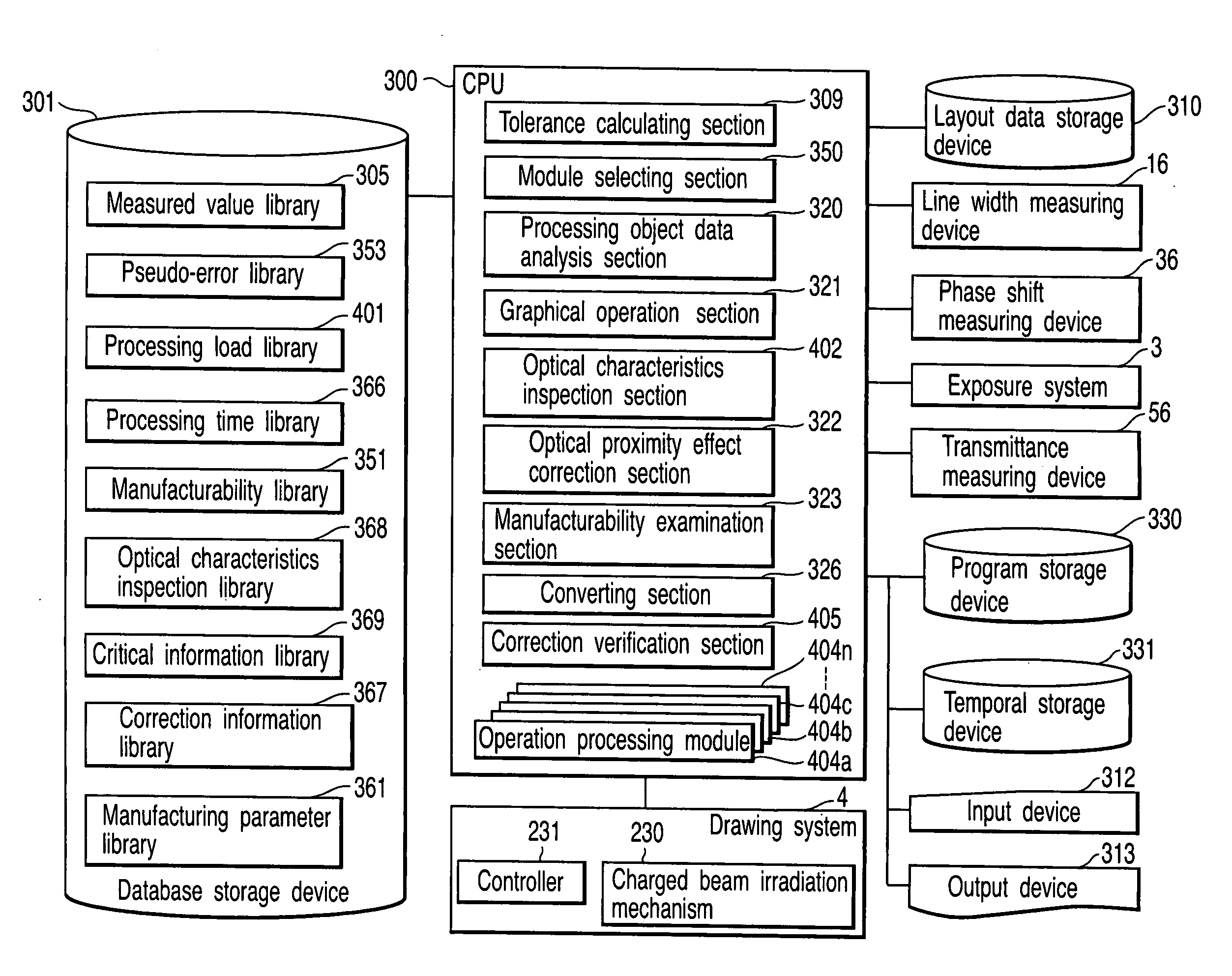
[0024]FIG. 1 shows an example of a cell diagram of a mask manufacturing system according to an embodiment of the present invention. As shown in FIG. 1, the mask manufacturing system according to this embodiment comprises a central processing unit (CPU) 300, ...


PUM

PropertyMeasurementUnit
wavelengthaaaaaaaaaa
optical proximityaaaaaaaaaa
optical characteristics inspectionaaaaaaaaaa

Abstract

A mask manufacturing system and a mask data creating method reusing data for processing information and environment in the past to reduce a photomask developing period, and a manufacturing method of a semiconductor device are disclosed. According to one aspect of the present invention, it is provided a mask manufacturing system comprising a storage device storing processing data for semiconductor integrated circuits processed in the past, a plurality of operation processing modules, a module selecting section selecting at least one operation processing modules, an optical proximity effect correction section executing optical proximity effect correction to a processing object data and generating a correction data by utilizing past correction information applied for a stored data equivalent to the processing object data, a converting section converting the processing object data into mask data, and a drawing system drawing a mask pattern based on the mask data.

Description

CROSS-REFERENCE TO RELATED APPLICATIONS [0001] This application is based upon and claims the benefit of priority from prior Japanese Patent Application No. 2005-152830, filed May 25, 2005, the entire contents of which are incorporated herein by reference. BACKGROUND OF THE INVENTION [0002] 1. Field of the Invention [0003] The present invention relates to a mask data design environment of a semiconductor device manufacturing technology, and more particularly to a mask manufacturing system, a mask data creating method and a manufacturing method of a semiconductor device. [0004] 2. Description of the Related Art [0005] A degree of integration of a semiconductor integrated circuit is increasing from year to year, and miniaturization of design rules is also advancing. With advancement of miniaturization, an optical proximity effect (OPE) that a layout pattern is not accurately transferred onto a wafer has become a problem. Therefore, there has been proposed an optical proximity effect co...

Claims


Application Information

Patent Timeline
Patent Type & Authority Applications(United States)
IPC IPC(8): G06F17/50G03F1/36G03F1/68
CPCG03F1/144G03F1/36G03F1/68
Inventor KOBAYASHI, SACHIKOKOTANI, TOSHIYA
Owner KK TOSHIBA
Why Eureka
Try Eureka