

Tape carrier package and display device including tape carrier package
- Summary
- Abstract
- Description
- Claims
- Application Information
AI Technical Summary
Benefits of technology
Problems solved by technology
Method used
Image

Examples
first example
[0064] A tape carrier package according to a first example of the present invention will be described using drawings.
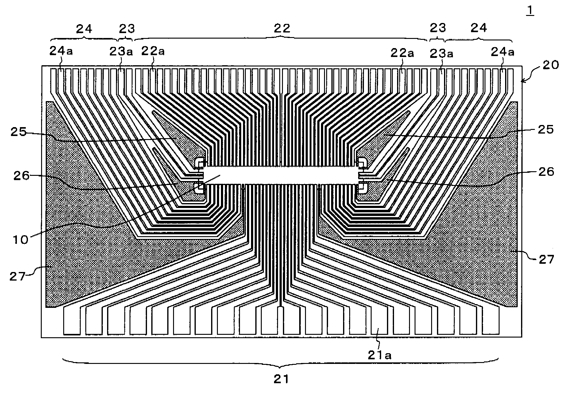
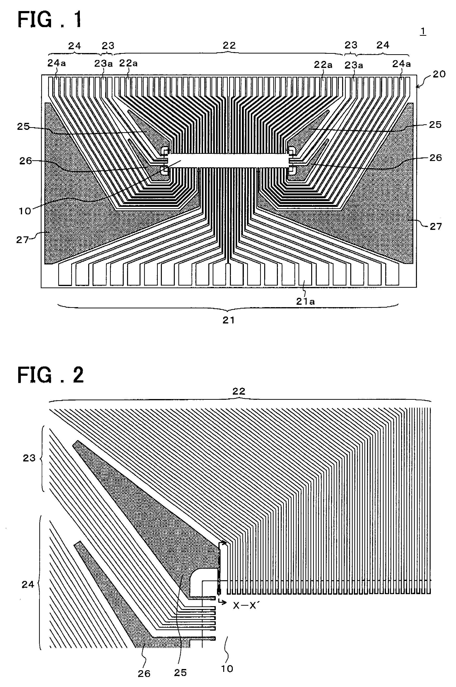
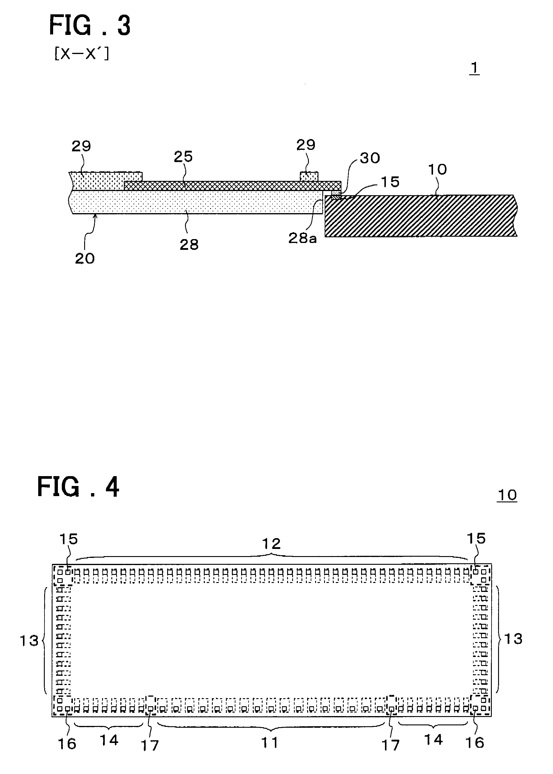
[0065]FIG. 1 is a plan view schematically showing a configuration of the tape carrier package according to the first example of the present invention. FIG. 2 is a partially enlarged plan view schematically showing the configuration of the tape carrier package according to the first example of the present invention. FIG. 3 is a partially enlarged sectional view taken along line X-X′ in FIG. 2 and schematically showing the configuration of the tape carrier package according to the first example of the present invention. FIG. 4 is a plan view schematically showing electrode patterns in the tape carrier package according to the first example of the present invention.
[0066] Referring to FIG. 1, a tape carrier package 1 is a tape carrier package which is mounted on a display panel (not shown) such as a liquid crystal display, a plasma display, or the like, and which inclu...
second example
[0087] A tape carrier package according to a second example of the present invention will be described, using a drawing. FIG. 5 is a plan view schematically showing a configuration of the tape carrier package according to the second example of the present invention.
[0088] In the tape carrier package 1 according to the second example a grounding or signal external electrode 27a is provided at each heat dissipation pattern 27. Other configurations are the same as those in FIG. 1.
[0089] The heat dissipation patterns 27 are heat dissipation patterns which are formed on the backsurface of the tape base 28 and are each made of an electro-conductive material such as the copper foil (e.g. the tin-plated copper base material, or the gold-plated copper base material). Each of the heat dissipation patterns 27 is disposed in the region between an outermost one of (a group of) the lead patterns 24 and an outermost one of (a group of) the lead patterns 21. An end of the heat dissipation pattern...
third example
[0093] A tape carrier package according to a third example of the present invention will be described, using a drawing. FIG. 6 is a plan view schematically showing a configuration of the tape carrier package according to the third example of the present invention.
[0094] In the tape carrier 20 of the tape carrier package I according to the third example, the heat dissipation patterns (indicated by reference numeral 27 in FIGS. 1 and 5) and the lead patterns (indicated by reference numeral 24 in FIGS. 1 and 5) like those in the first and second examples are omitted. Areas of the heat dissipation patterns 26 are increased, and the (second) heat dissipation patterns 26 are provided in spaces which have become unoccupied by the omission. A grounding or signal external electrode 26a is provided at each of the heat dissipation patterns 26. The semiconductor device 10 does not have the electrode pattern (indicated by reference numeral 14 in FIG. 4) and the heat dissipating electrode patter...
PUM
 Abstract
Description
Claims
Application Information