
Electronic device

Inactive Publication Date: 2007-06-07
TOYO TSUSHINKI
View PDF4 Cites 24 Cited by
  • Summary
  • Abstract
  • Description
  • Claims
  • Application Information

AI Technical Summary

Benefits of technology

[0012] An advantage of the present invention is to provide an electronic device capable of reliably inputting a signal to an electronic component arranged thereinside and preventing alteration and deletion of the signal written into the electronic component, where a cover has a constant potential in normal use.
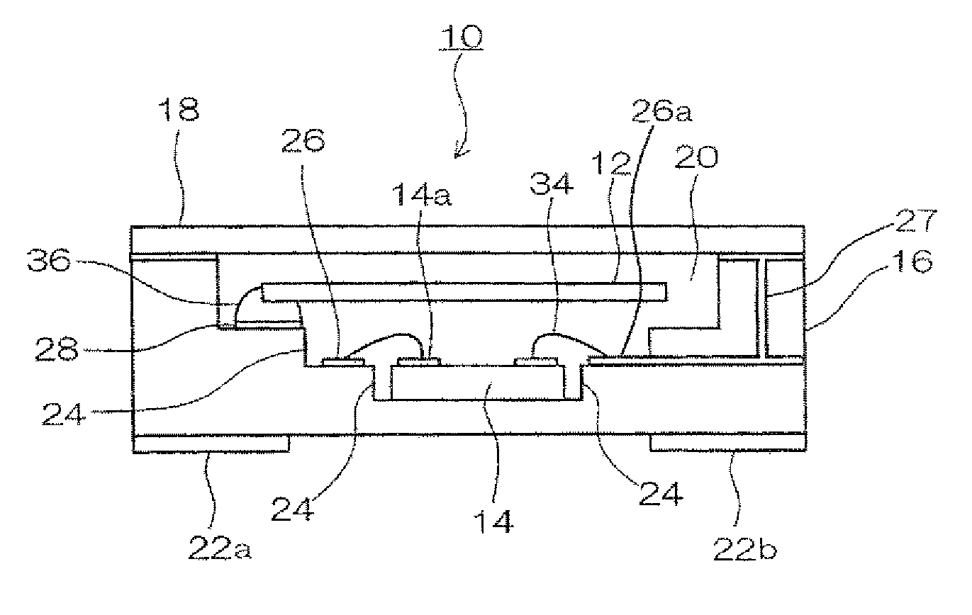
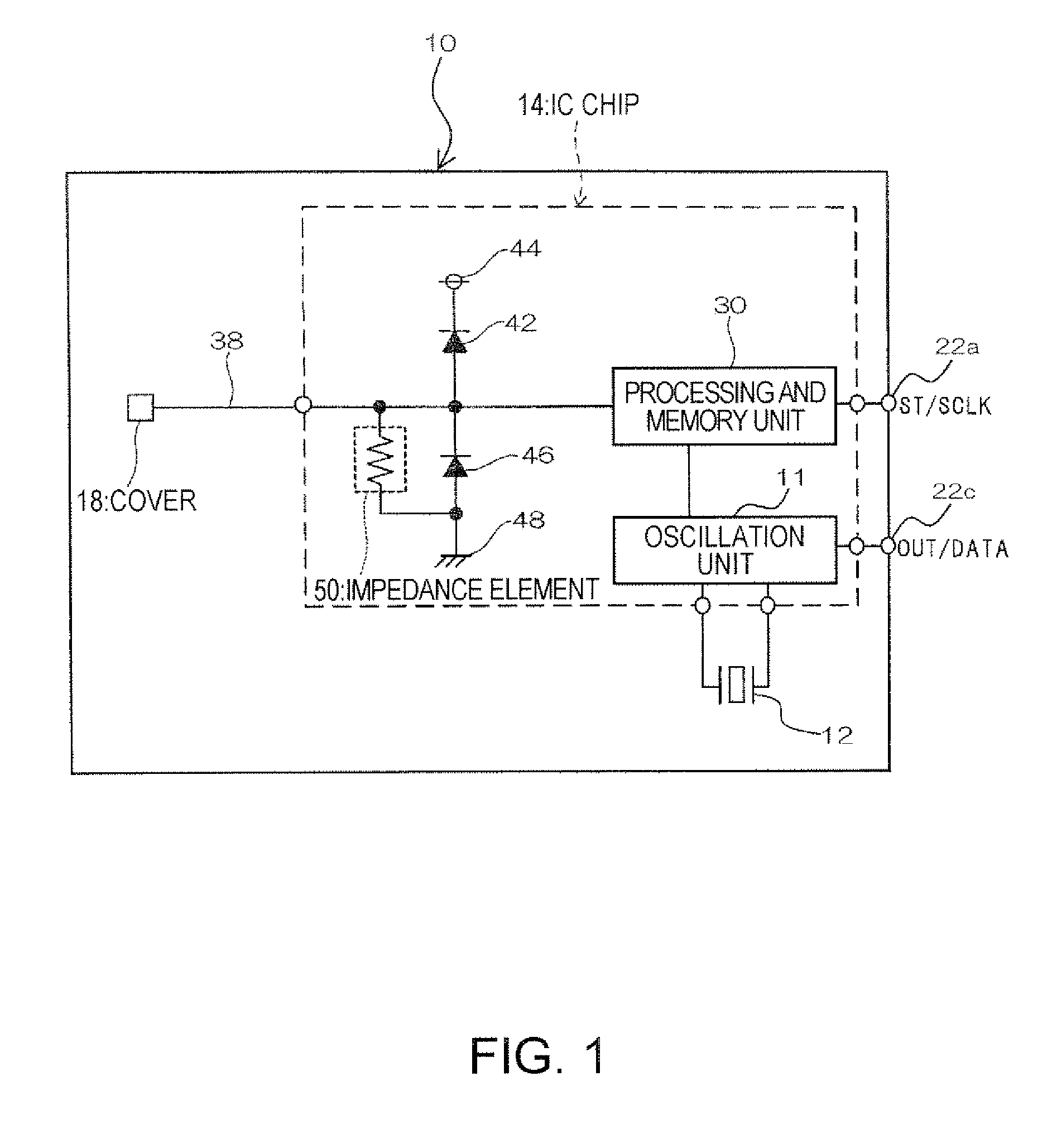
[0013] An electronic device according to one aspect of the invention includes an electronic component, a package base having the electronic component therein and a conductive cover bonded to the package base, wherein a signal transmission line is provided to electrically connect the cover to the electronic component so as to use the cover as a terminal for inputting a signal to the electronic component from outside; and wherein the signal transmission line is connected to a constant potential portion via an impedance element.
[0014] In this manner, the cover can be connected to the constant potential portion via the impedance element. Thus, a signal input from the cover can be input to the electronic component via the signal transmission line. Meanwhile, in a normal use situation when no signal is input, the cover is connected to the constant potential portion via the impedance device. Accordingly, since the potential of the cover can be held constant, alteration and deletion of the signal written into the electronic component can be prevented. In addition, since the cover serves as the terminal to which a signal is input, a probe supplying a signal can easily be contacted with the cover, thereby ensuring signal input precisely.
[0015] Furthermore, the impedance element may be integrally formed with the electronic component. In this manner, since the impedance element is arranged inside the electronic component, it is unnecessary to dispose the impedance element as a discrete component in the package base. Thus, space saving in the package base can be achieved.
[0016] Furthermore, the package base may have the impedance element therein. When the in-use electronic component or package base has the impedance device therein, the cover can be connected to the constant potential portion when no signal is input to the electronic component. Consequently, alternation and deletion of the signal input to the electronic component can be prevented.
[0017] Furthermore, the constant potential portion may be a grounded portion. In this manner, the potential of the cover can be fixed at a ground potential.

Problems solved by technology

Accordingly, there arises a problem of changing an oscillation frequency of the piezoelectric oscillator.
However, if the container has a dent made therein due to a shock or the like for some reason, there is a possibility that the container may contact with the cover of the piezoelectric oscillator.
However, even in this piezoelectric oscillator, when a plurality of electrodes is arranged on an external side surface of the package base to input data to an IC chip, a malfunction is likely to occur upon data input.
However, it is a difficult task to allow the probes to accurately contact with the electrodes arranged on the side surface.
Therefore, a malfunction such as a data input failure occurs due to a poor contact.
Thus, when an electric signal is loaded due to an accidental contact of a piezoelectric oscillator with any of electronic devices adjacent thereto, it can cause alteration or deletion of data written into an IC chip in the piezoelectric oscillator.

Method used


Image

  • Electronic device
  • Electronic device
  • Electronic device

Examples


second embodiment

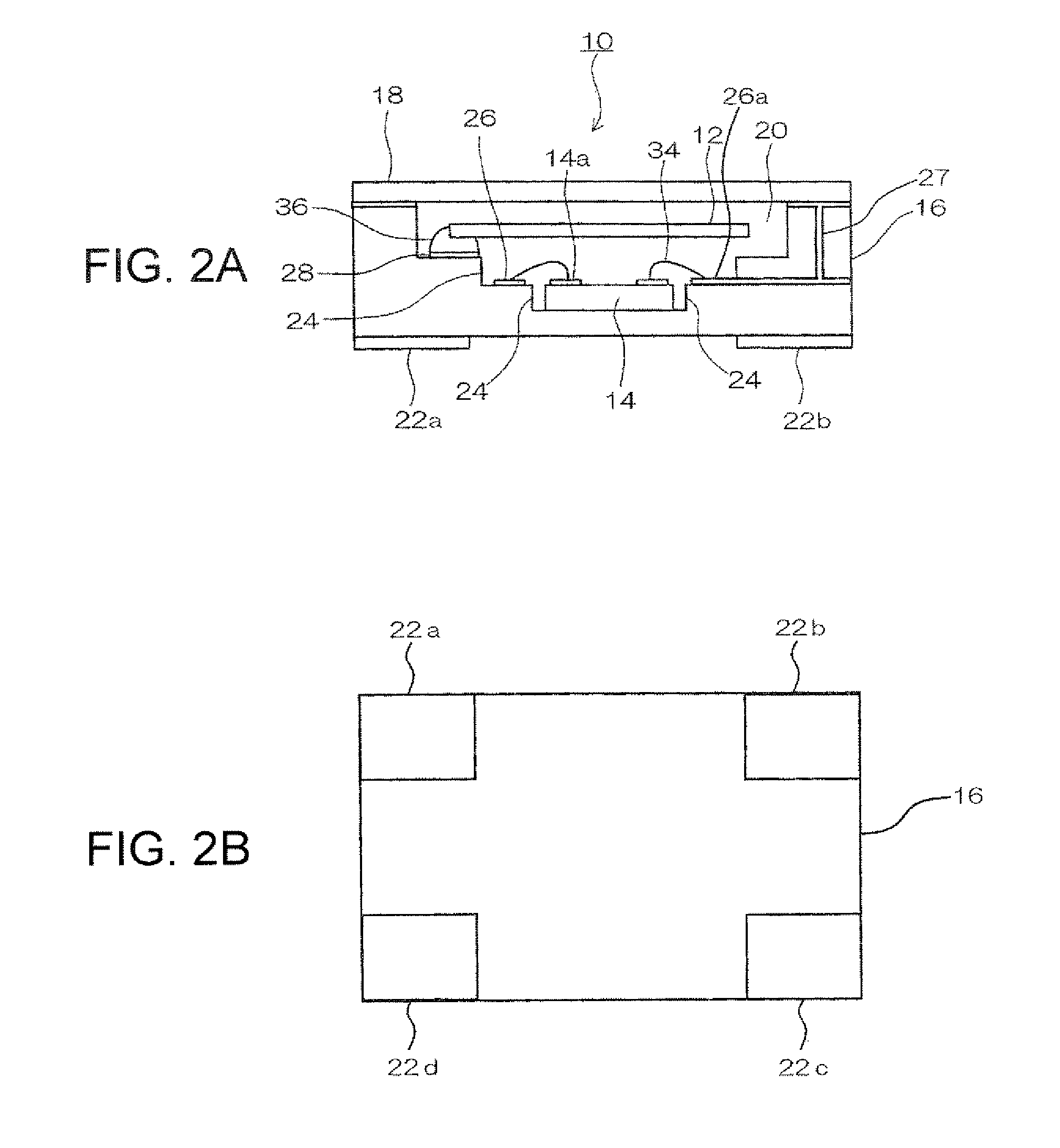
[0057] In the above package base 16, the impedance element 503 is mounted above the bonding electrode 26h electrically connected to the cover 18 and the bonding electrode 26g electrically connected to the grounded external terminal 22b. Thus, the bonding electrodes 26g and 26h are electrically connected to each other via the impedance element 503. The recessed portion 20 has the IC chip 14 on the bottom surface thereof. A wire bonding is provided on the pad 14a disposed on the IC chip 14 and the bonding electrodes 26a to 26f and 26h to electrically connect them via the wire 34. The IC chip 14 employed in the second embodiment is similar to that shown in FIG. 1, but does not include an impedance element.

first embodiment

[0058] Additionally, the piezoelectric resonator element 12 is mounted above the mount electrode 28 in the same manner as shown in FIG. 2A. Also, the cover 18 is bonded onto the package base 16 to airtightly seal the recessed portion 20 in the same manner as shown in FIG. 2A. In the above piezoelectric oscillator 102, data writing can be performed in the same manner as that of the

[0059] Furthermore, the package base 16 of the piezoelectric oscillator 102 has the impedance element 50 therein. Thus, the cover 18 can have a constant potential. When mounting the piezoelectric oscillator 102 on a substrate of an electronic apparatus, regardless of the use situations on the user side, oscillation-frequency fluctuations due to the influence of stray capacitance can be prevented, because the cover 18 of the piezoelectric oscillator 102 is grounded via the impedance element 503.

[0060] Since the cover 18 is also grounded via the impedance element 50, an electrostatic buildup can be prevented...

third embodiment

[0065] The switching circuit 70 connects the cover 18 to the processing and memory unit 30 of the piezoelectric oscillator 103 so that the cover 18 can input a signal to the processing and memory unit 30 when data is written into the processing and memory unit 30 thereof. Additionally, the switching circuit 70 connects the cover 18 to the grounded portion 48 in a normal use situation when the piezoelectric oscillator 103 outputs an oscillation signal. In the third embodiment, when a voltage level of a signal input to the cover 18 is lower than a predetermined voltage level Vth, the switching circuit 70 connects the cover 18 to the grounded portion 48, whereas it connects the cover 18 to the processing and memory unit 30 when the voltage level of the input signal is equal to or higher than the predetermined voltage Vth.

[0066] Next, a detailed explanation will be given of the switching circuit 70. FIG. 9 is an illustrative view of the switching circuit 70. In this circuit, a first res...


PUM


Abstract

An electronic device includes an electronic component, a package base having the electronic component therein and a conductive cover bonded to the package base, wherein a signal transmission line is provided to electrically connect the cover to the electronic component so as to use the cover as a terminal for inputting a signal to the electronic component from outside and wherein the signal transmission line is connected to a constant potential portion via an impedance element.

Description

BACKGROUND [0001] 1. Technical Field [0002] The present invention relates to an electronic device, particularly to an electronic device in which a signal is input to an electronic component arranged therein after the formation of the electronic device. [0003] 2. Related Art [0004] Some electronic devices have a package base with a recessed portion formed therein. The recessed portion has an electronic component mounted on a bottom surface thereof and a cover is bonded onto a top surface of the package base to seal the recessed portion. One example of such electronic devices is a piezoelectric oscillator. The piezoelectric oscillator has a package base in which a piezoelectric resonator element is disposed opposing the cover and an integrated circuit (IC) chip is provided as an electronic component to oscillate the piezoelectric resonator element to output a high-frequency oscillation signal. The piezoelectric resonator element is comprised of an electrode pattern disposed on each of...

Claims


Application Information

Patent Timeline
IPC IPC(8): H01L41/00H01L23/02H01L23/48H01L23/12
CPCH03H9/0547H03H9/1021H01L2224/05554H01L2224/48091H01L2224/48227H01L2224/49171H01L2924/16195H01L2924/00014
Inventor USUDA, TOSHIYAKINOSHITA, HIROSHI
Owner TOYO TSUSHINKI
Learn More