Digital-to-analog converter, data driver and display device using same

a digital-to-analog converter and data driver technology, applied in the direction of digital-analog converters, transmission systems, instruments, etc., can solve the problems of increasing the chip area of the data driver lsi chip, increasing the number of bits of video data, increasing the cost, etc., and achieving the effect of reducing the area and reducing the cos

Inactive Publication Date: 2007-06-07
NEC CORP
View PDF6 Cites 26 Cited by
  • Summary
  • Abstract
  • Description
  • Claims
  • Application Information

AI Technical Summary

Benefits of technology

[0039] The present invention is such that in a DAC using a differential amplifier having n input voltages and capable of outputting a voltage obtained by taking the weighted mean of these voltages at a ratio of 2n−1:2n−2: . . . :20, an advantage is that a maximum of mn voltage levels can be output with respect to the number m of voltages received by the DAC.
[0040] In accordance with the present invention, the effect of reducing area is significant and cost can be reduced in fields where there is a very large number of bits, as in the data driver of a liquid crystal display device, etc.

Problems solved by technology

These invite an increase in cost.
Accordingly, an increase in the number of bits of video data increases the chip area of the data driver LSI chip and raises cost.

Method used


Image

  • Digital-to-analog converter, data driver and display device using same
  • Digital-to-analog converter, data driver and display device using same
  • Digital-to-analog converter, data driver and display device using same

Examples


second embodiment

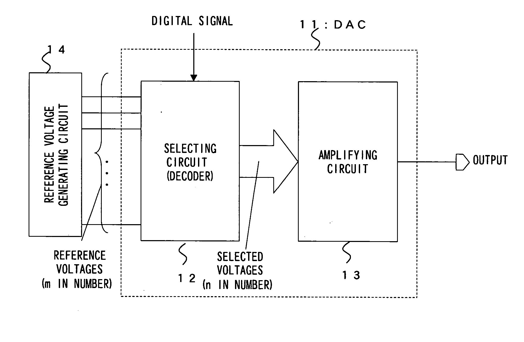
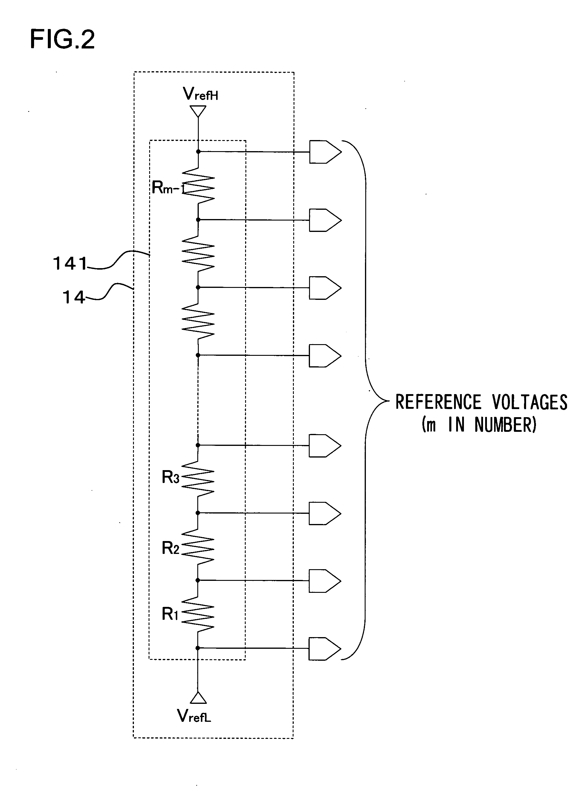
[0122] Next, a case where the decoder 12 of FIG. 1 has n output terminals (i.e., where the amplifying circuit 13 has n input terminals) will be described as the present invention. That is, the decoder 12 receives m reference voltages that differ from one another, selects n voltages, inclusive of voltages that may be identical, from among the m reference voltages based upon a selecting signal, and supplies the selected voltages to n output terminals T1, T2, . . . , Tn.

[0123] Further, the amplifying circuit 13 outputs a voltage obtained by taking the weighted mean of the n voltages, which have been supplied to the terminals T1 to Tn, at a ratio of 2n−1:2n−2: . . . :20. Let VQ1, VQ2, . . . , and VQn represent the n voltages supplied to the terminals T1 to Tn.

[0124] A case where there are four reference voltages and three output terminals T1, T2 and T3 of the decoder 12, namely a case where m=4, n=3 holds, will now be described as an example. FIG. 31 is a diagram illustrating the relat...

third embodiment

[0186] Next, a case where the decoder 12 in FIG. 1 has a single output terminal (the amplifying circuit 13 has a single input terminal) will be described as the present invention. That is, the decoder 12 receives as inputs the m reference voltages that differ from one another, selects n voltages, inclusive of voltages that may be identical, from among the m reference voltages based upon a selecting signal, and successively outputs the selected voltages to a single output terminal. Further, the amplifying circuit 13 successively receives as inputs the n voltages selected at the single output terminal and outputs voltages obtained by taking the weighted mean of the entered n voltages at the ratio 2n−1:2n−2: . . . :20. The single output terminal will be expressed by T0 below, and the n voltages successively supplied to the terminal T0 will be denoted by VQ1, VQ2, . . . , and VQn.

[0187]FIG. 19A is a diagram illustrating an example of the configuration of the amplifying circuit 13 accord...

fourth embodiment

[0238] Next, a case where the decoder 12 of FIG. 1 has r (213 has r input terminals) will be described as the present invention. That is, the decoder 12 receives as inputs the m reference voltages that differ from one another, selects n voltages, inclusive of voltages that may be identical, from among the m reference voltages based upon a selecting signal, and successively outputs the selected voltages to r output terminals.

[0239] Further, the amplifying circuit 13 successively receives as inputs the n voltages selected at the r output terminals and outputs voltages obtained by taking the weighted mean of the entered n voltages at the ratio 2−1:2n−2: . . . :20. The r output terminals will be expressed by T0 to Tr below, and the n voltages successively supplied to the terminals T0 to Tr will be denoted by VQ1, VQ2, . . . , and VQn, respectively.

[0240]FIG. 24A is a diagram illustrating an example of the configuration of the amplifying circuit 13 according to this embodiment, and FIG....


PUM


Abstract

Disclosed is a digital-to-analog converter including a decoder which receives m (where m>=4 holds) reference voltages having voltage values that differ from one another, and selects and outputs n (where n>=3 holds) identical or different voltages from among the m reference voltages based upon a digital signal; and an amplifying circuit that outputs a voltage, which is obtained by taking the weighted mean of the selected n voltages at a ratio of 2n−1:2n−2: . . . :20, from an output terminal.

Description

FIELD OF THE INVENTION [0001] This invention relates to a digital-to-analog converter and to a data driver and display device that employ this converter. BACKGROUND OF THE INVENTION [0002] Liquid crystal display devices (LCDs) characterized by their thin design, light weight and low power consumption have come into widespread use in recent years and are utilized in the display units of mobile devices such as portable telephones (mobile telephones or cellular telephones), PDAs (Personal Digital Assistants) and laptop personal computers. Recently, however, liquid crystal display devices have come to be provided with large-size screens and techniques for dealing with moving pictures have become more advanced, thus making it possible to realize not only mobile applications but also stay-at-home large-screen display devices and large-screen liquid crystal televisions. Liquid crystal display devices that rely upon active matrix drive and are capable of presenting a high-definition display...

Claims


Application Information

Patent Timeline
Patent Type & Authority Applications(United States)
IPC IPC(8): G09G3/36
CPCG09G3/2011G09G3/3688H03M1/76G09G2320/0276H03M1/0646G09G2310/027
Inventor ISHII, JUNICHIROTSUCHI, HIROSHI
Owner NEC CORP
Why Eureka
Try Eureka