High voltage CMOS devices

a high-voltage semiconductor and gate length technology, applied in the field of semiconductor devices, can solve the problems of device failure, short gate length, and short gate length, and achieve the effect of efficient and cost-effectiv

Active Publication Date: 2007-06-14
TAIWAN SEMICON MFG CO LTD
View PDF11 Cites 100 Cited by
  • Summary
  • Abstract
  • Description
  • Claims
  • Application Information

AI Technical Summary

Benefits of technology

[0011] The first and / or second well may be formed simultaneously as forming a similar well in a low-voltage region for a low-voltage transistor. In this manner, low-voltage transistors and high-voltage transistors may be fabricated in an efficient and cost-effective manner.

Problems solved by technology

The use of higher voltages with shorter gate length MOSFETs, however, may create undesirable effects, such as punch-through.
Generally, punch-through occurs when an electrical connection is formed between different regions during high-voltage operation, possibly creating a short condition between the two regions causing the device to fail.
This process, however, is time-consuming, expensive, and generally requires additional process steps.
For example, the epitaxial layer is a time-consuming process and reduces the amount of units that may be produced within a given amount of time.
Accordingly, particularly in designs in which it is desirable to utilize low-voltage and high-voltage devices on a single substrate, high-voltage devices typically require additional processing steps and longer processing times.

Method used


Image

  • High voltage CMOS devices
  • High voltage CMOS devices
  • High voltage CMOS devices

Examples


Embodiment Construction

[0025] The making and using of the presently preferred embodiments are discussed in detail below. It should be appreciated, however, that the present invention provides many applicable inventive concepts that can be embodied in a wide variety of specific contexts. The specific embodiments discussed are merely illustrative of specific ways to make and use the invention, and do not limit the scope of the invention.

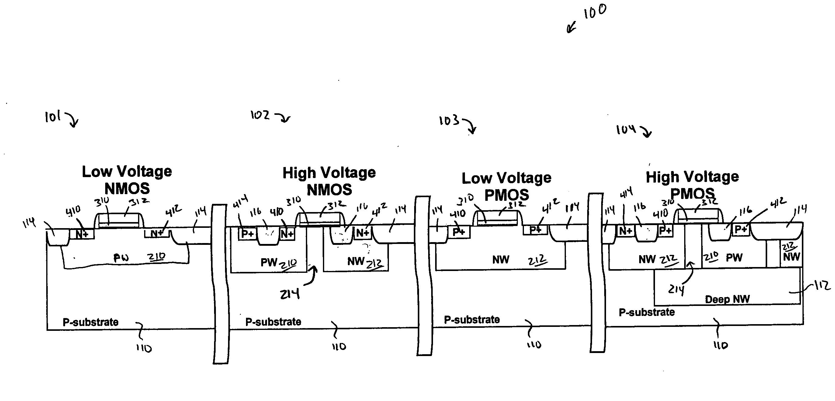
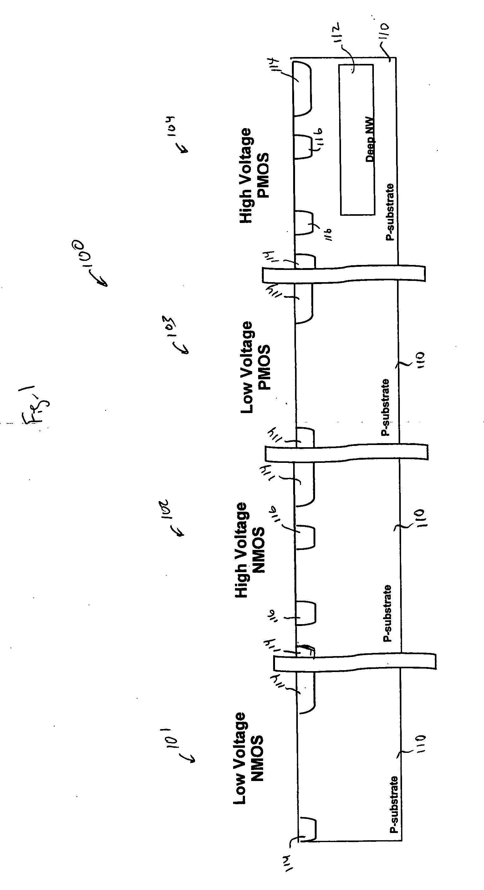
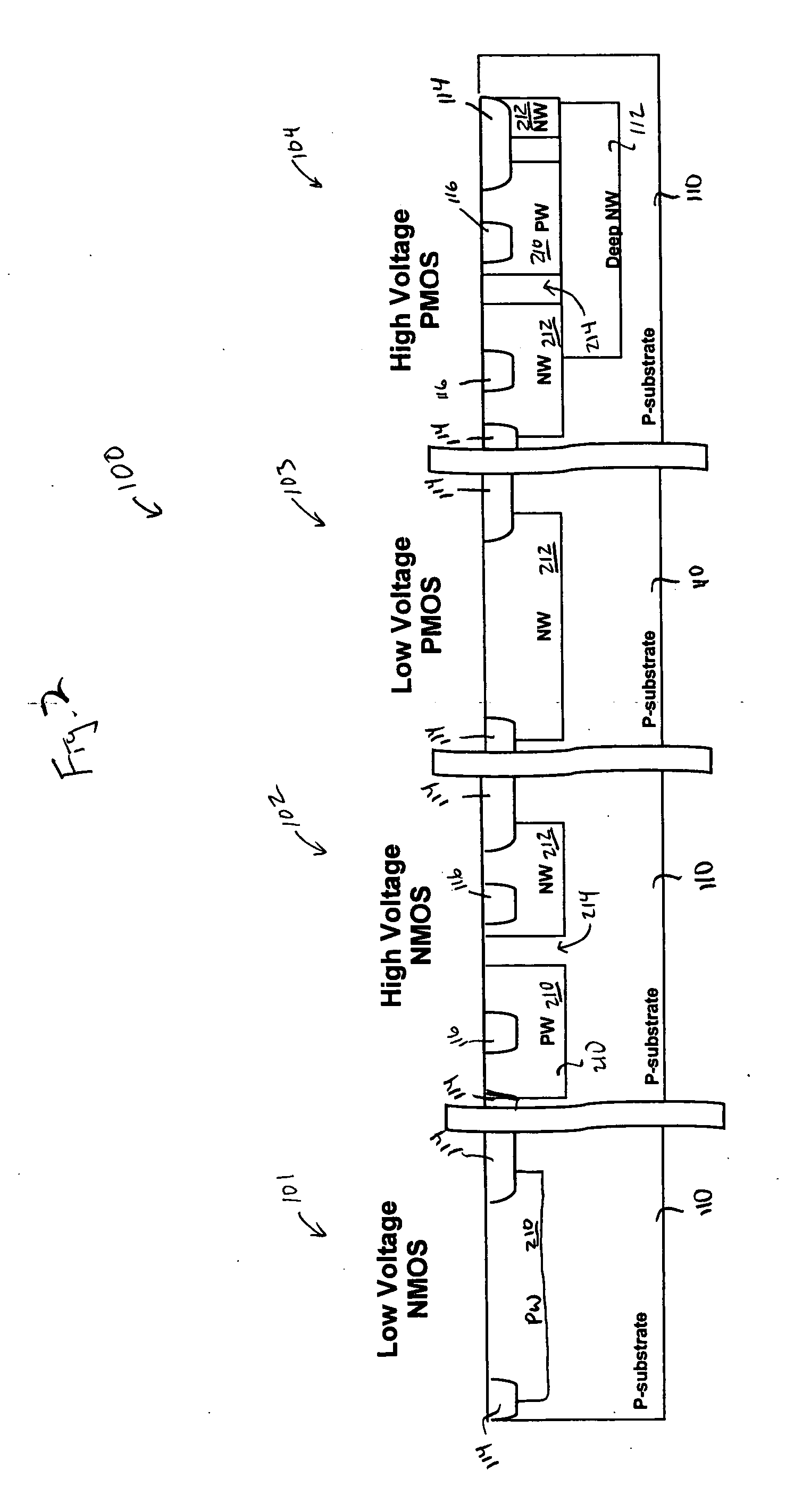
[0026]FIGS. 1-4 illustrate various stages of fabricating a semiconductor device having high-voltage PMOS and NMOS transistors and low-voltage PMOS and NMOS transistors in accordance with an embodiment of the present invention. It should be noted that the following method illustrates the formation of one of each of these transistors for illustrative purposes only, and embodiments of the present invention may be used to fabricate semiconductor devices having any combination of one or more these transistors. A high-voltage transistor includes transistors expecting more than ab...


PUM


Abstract

A transistor suitable for high-voltage applications is provided. The transistor is formed on a substrate having a deep well of a first conductivity type. A first well of the first conductivity type and a second well of a second conductivity type are formed such that they are not immediately adjacent each other. The well of the first conductivity type and the second conductivity type may be formed simultaneously as respective wells for low-voltage devices. In this manner, the high-voltage devices may be formed on the same wafer as low-voltage devices with fewer process steps, thereby reducing costs and process time. A doped isolation well may be formed adjacent the first well on an opposing side from the second well to provide further device isolation.

Description

TECHNICAL FIELD [0001] The present invention relates generally to semiconductor devices and, more particularly, to high-voltage semiconductor devices. BACKGROUND [0002] Size reduction of complementary metal-oxide-semiconductor (CMOS) devices, such as transistors, has enabled the continued improvement in speed, performance, density, and cost per unit function of integrated circuits over the past few decades. As sizes are reduced, there has been a trend to integrate more functions on a single chip, some of which require higher voltage levels. The use of higher voltages with shorter gate length MOSFETs, however, may create undesirable effects, such as punch-through. [0003] Generally, punch-through occurs when an electrical connection is formed between different regions during high-voltage operation, possibly creating a short condition between the two regions causing the device to fail. One attempt to solve this problem utilizes a barrier layer formed along a surface of a substrate. An ...

Claims


Application Information

Patent Timeline
Patent Type & Authority Applications(United States)
IPC IPC(8): H01L29/76
CPCH01L21/823814H01L21/823892H01L27/092H01L29/0653H01L29/0847H01L29/1083H01L29/7835H01L29/7816H01L29/0852
Inventor WU, CHEN-BAUTANG, CHIEN-SHAOHSIEH, ROBINLIU, RUEY-HSINHSU, SHUN-LIANG
Owner TAIWAN SEMICON MFG CO LTD
Why Eureka
Try Eureka