Method And Apparatus For Switching Audio And Data Signals Through A Single Terminal
a single terminal and audio and data technology, applied in electronic switching, pulse technique, semiconductor devices, etc., can solve the problems of high cost and substantial capacitance loading at the common terminal, distortion of audio signals, etc., and achieve the effect of reducing the occupancy area of semiconductor circuits, minimizing parasitic capacitance, and convenient switching
- Summary
- Abstract
- Description
- Claims
- Application Information
AI Technical Summary
Benefits of technology
Problems solved by technology
Method used
Image
Examples
first embodiment
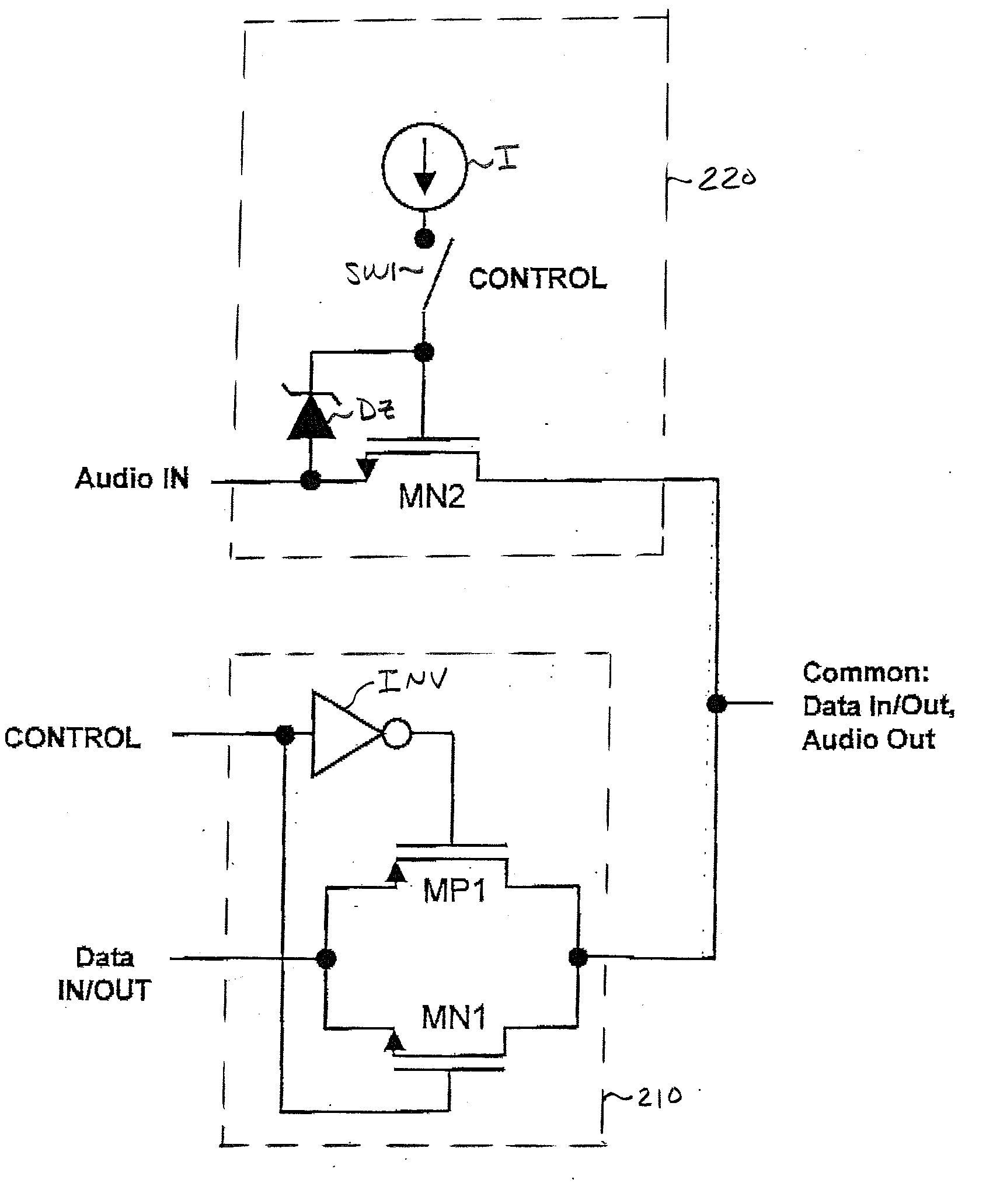
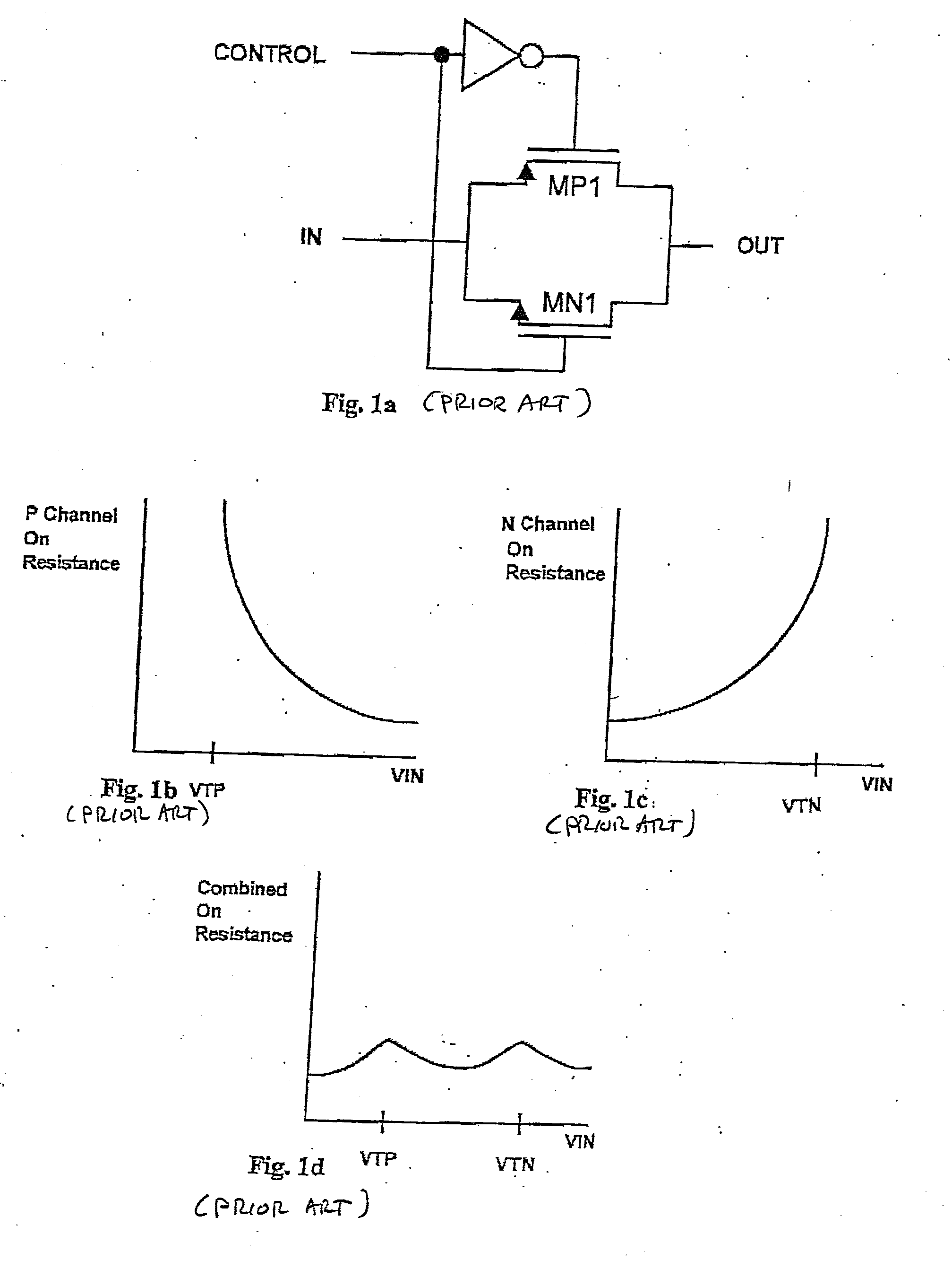
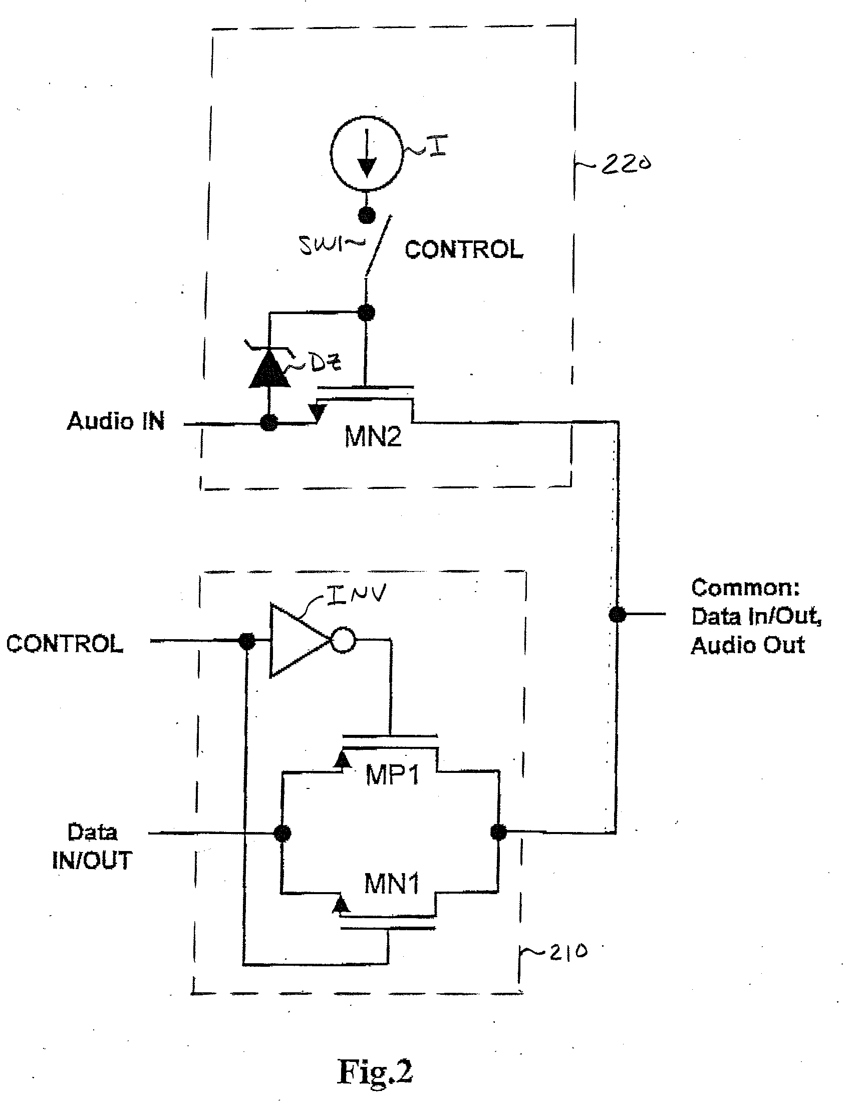
[0030] Attention is now directed to FIG. 2, which schematically illustrates the multi-signal SPDT switching circuit of the present invention, as a combination of a high speed data signal switch 210, which may be implemented by the CMOS switching circuit of FIG. 1a, and an auxiliary analog (e.g., audio) signal switch 220, which is implemented by a single NMOS transistor MN2, having its source-drain path coupled between an analog / audio input terminal / port ‘Audio In’ and the signalling interface terminal / port ‘Common’, through which analog / audio output signals, as well as data input and output signals, are coupled. As noted previously, porting both analog / audio and data signals to the same signalling interface terminal ‘Common’ allows the use of a single mechanical connector to pass high quality data signals into the device, thereby reducing size, weight and cost.
[0031] In the first embodiment of the invention shown in FIG. 2, the single analog / audio signal switching N-channel MOSFET M...
second embodiment
[0033]FIG. 3 schematically illustrates the multi-signal SPDT switching circuit of the invention, wherein the gate-to-source voltage-clamping Zener diode Dz of the audio signal switch 220 of the embodiment of FIG. 2 is replaced by a gate-to-source coupling resistor R. The multi-signal switching circuit of FIG. 3 is otherwise the same as that of FIG. 2. The injection of a constant bias current from the constant current source I through the gate-to-source coupling resistor R for the ON state of the switching MOSFET MN2 sets the gate-to-source bias voltage VGS of MOSFET MN2 at a constant value, corresponding to the product of the coupling resistance R and the value of the constant current I. This allows the multi-signal switching circuit of FIG. 3 to offer the same advantages as the implementation of FIG. 2, over using two of the conventional signal CMOS-based analog signal switching circuits of FIG. 1a for respective audio and digital signaling paths to implement the desired SPDT switc...
third embodiment
[0034]FIG. 4 schematically illustrates the multi-signal SPDT switching circuit of the invention, wherein the Zener diode Dz and the resistor R of the audio signal switch 220 of the respective multi-signal switching circuits of the embodiments of FIGS. 2 and 3 are replaced by a gate-to-source biasing N-channel MOSFET MN3. MOSFET MN3 has its drain and gate connected in common through the switch SW1 to the constant current source I, and its source coupled to the source of the N-channel MOSFET switch MN2. As a result, with switch SW1 being closed for the ON state of the analog / audio signal switching MOSFET MN2, MOSFET MN3 will provide the desired constant gate-to-source voltage for the switching MOSFET MN2.
[0035] The use of an N-channel MOSFET as the gate-to-source biasing component in the embodiment of the multi-signal SPDT switching circuit of FIG. 4 offers an improvement over the switching circuit embodiments of FIGS. 2 and 3, since parameters of the N-channel gate-to-source biasing ...
PUM
 Abstract
Description
Claims
Application Information


