Self-aligned vertical PNP transistor for high performance SiGe CBiCMOS process

a technology of bicmos and cbicmos, which is applied in the direction of transistors, solid-state devices, electric devices, etc., can solve the problems of poor performance of conventional bicmos gate circuits, composite bicmos buffers and npn output drivers, and achieve the effect of reducing repetition

Active Publication Date: 2007-06-14
CHARTERED SEMICONDUCTOR MANUFACTURING
View PDF9 Cites 66 Cited by
  • Summary
  • Abstract
  • Description
  • Claims
  • Application Information

AI Technical Summary

Benefits of technology

[0052] The above advantages and features are of representative embodiments only, and are not exhaustive and/or exclusive. They are presented only to assist in understanding the invention. It should be understood that they are not representative of all the inventions defined by the claims, to be considered limitations on the invention as defined by the claims, or limitations on equivalents to the claims. For instance, some of these advantages may be mutually contradictory, in that they cannot be simultaneously present in a single embodiment. Similarly, some advantages are

Problems solved by technology

However, the performance of conventional BiCMOS gate circuit, which is composi

Method used


Image

  • Self-aligned vertical PNP transistor for high performance SiGe CBiCMOS process
  • Self-aligned vertical PNP transistor for high performance SiGe CBiCMOS process
  • Self-aligned vertical PNP transistor for high performance SiGe CBiCMOS process

Examples


Embodiment Construction

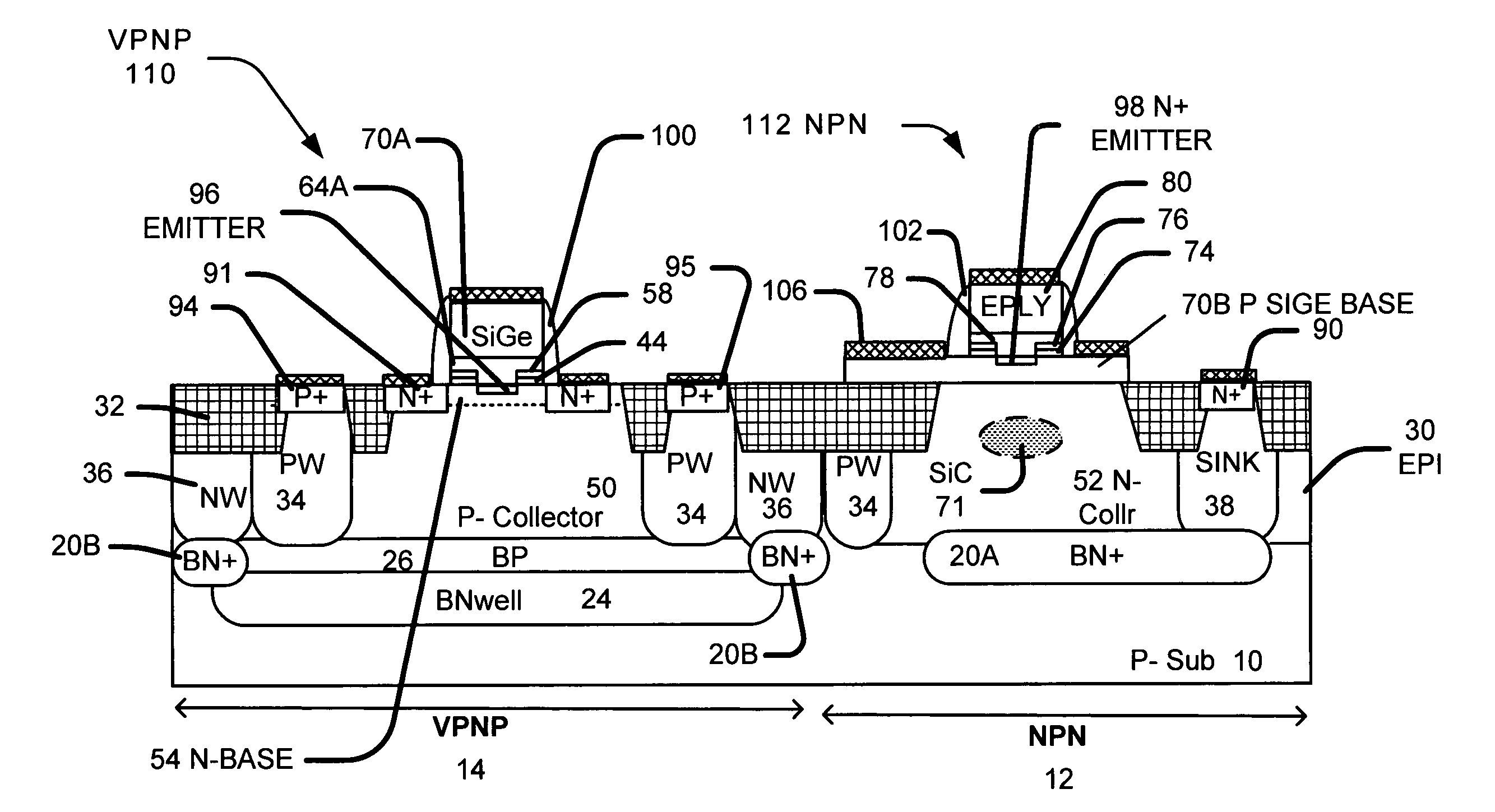
[0057] Example embodiments of the present invention will be described in detail with reference to the accompanying drawings. Example embodiments provide a structure and a method of forming a Self-Aligned Vertical PNP Transistor for High Performance SiGe CBiCMOS Process. FIG. 14 shows a cross sectional view of the transistor. In addition CMOS devices can be simultaneously formed.

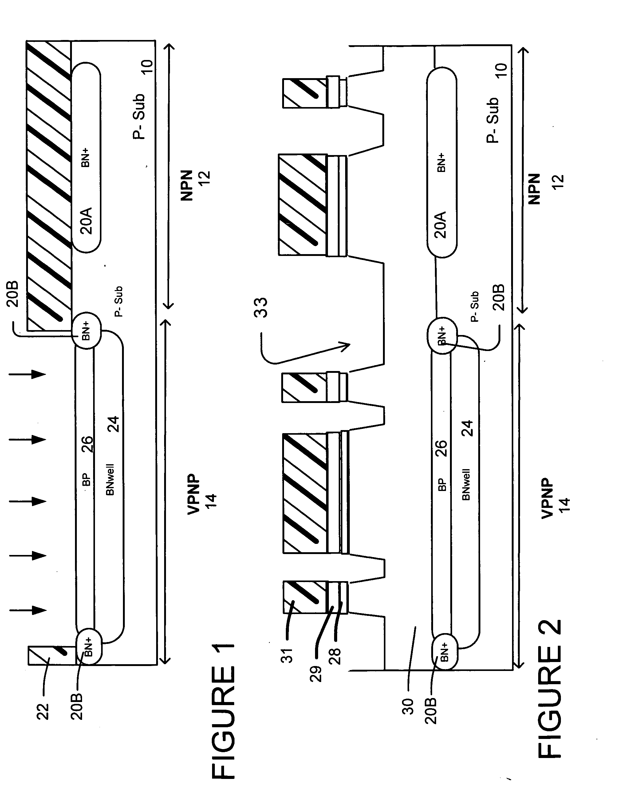
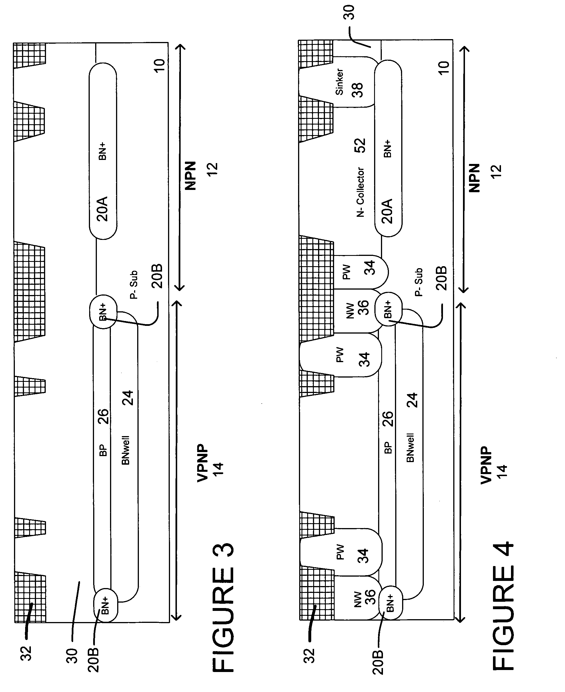
[0058] With reference to the accompanying drawings, FIGS. 1-14 illustrate fabrication process steps. Throughout the drawings, an NPN region 12 in which a vertical NPN transistor will be created is shown on the right, and a VPNP region 14 in which a vertical PNP transistor will be created is shown on the left. It should be recognized that some of the steps of fabrication according to conventional SiGe technology have been omitted for brevity and clarity.

[0059] An example method to form the vertical PNP Transistor for SiGe CBiCMOS process as shown in FIGS. 1 to 14.

[0060]FIG. 15B shows a schematic of a princi...


PUM


Abstract

A structure and a process for a self-aligned vertical PNP transistor for high performance SiGe CBiCMOS process. Embodiments include SiGe CBiCMOS with high-performance SiGe NPN transistors and PNP transistors. As the PNP transistors and NPN transistors contained different types of impurity profile, they need separate lithography and doping step for each transistor. The process is easy to integrate with existing CMOS process to save manufacturing time and cost. As plug-in module, fully integration with SiGe BiCMOS processes. High doping Polysilicon Emitter can increase hole injection efficiency from emitter to base, reduce emitter resistor, and form very shallow EB junction. Self-aligned N+ base implant can reduce base resistor and parasitical EB capacitor. Very low collector resistor benefits from BP layer. PNP transistor can be Isolated from other CMOS and NPN devices by BNwell, Nwell and BN+ junction.

Description

BACKGROUND OF INVENTION [0001] 1) Field of the Invention [0002] This invention relates generally to devices and the fabrication of semiconductor devices and more particularly to the fabrication of a vertical PNP transistors and methods for making same in BiCMOS processes. [0003] 2) Description of the Prior Art [0004] High speed and low-power LSIs, which operate in the GHz band, has been required for many applications such as the mobile telecommunication and wireless LNAs. The SiGe BiCMOS LSIs have been widely studied as potential candidate. However, the performance of conventional BiCMOS gate circuit, which is composite by CMOS buffer and NPN output driver is poor when the power supply is lower. This degradation at low power supply is due to the Vbe voltage loss and substrate bias effect of the CMOSFET (FIG. 15A). To overcome this problem, several BiCMOS circuits have been proposed. Adding high-speed PNP transistors into the SiGe BiCMOS to form so-called complementary BiCMOS (CBiCMO...

Claims


Application Information

Patent Timeline
IPC IPC(8): H01L21/8232H01L21/335
CPCH01L21/82285H01L21/8249H01L27/0623H01L27/0826H01L29/7378
Inventor ZHANG, SHAOQIANGVERMA, PURAKH RAJCHU, SANFORD
Owner CHARTERED SEMICONDUCTOR MANUFACTURING
Why Eureka
Try Eureka