Power ldmos transistor

a technology of mos transistor and mos, which is applied in the direction of basic electric elements, electrical equipment, and semiconductor devices, can solve the problems of difficult and often times more expensive design of mos transistors, narrow manufacturing tolerances of devices, and inability to meet the requirements of power management applications

Active Publication Date: 2007-06-21
TEXAS INSTR LEHIGH VALLEY
View PDF29 Cites 123 Cited by
  • Summary
  • Abstract
  • Description
  • Claims
  • Application Information

AI Technical Summary

Problems solved by technology

When used in PWM applications, the transistors must exhibit small power loss during switching, which imposes an additional requirement—small internal capacitances—that make the MOSFET design challenging and often times more expensive.
The thick epitaxial layer and P+ substrate result in a high on resistance (Rds,on) of the device, which is not acceptable for power management applications.
However, the breakdown voltage of the device is highly dependent on the location of the first portion of the drain region, which narrows the manufacturing tolerances for the device.

Method used


Image

  • Power ldmos transistor
  • Power ldmos transistor
  • Power ldmos transistor

Examples


Embodiment Construction

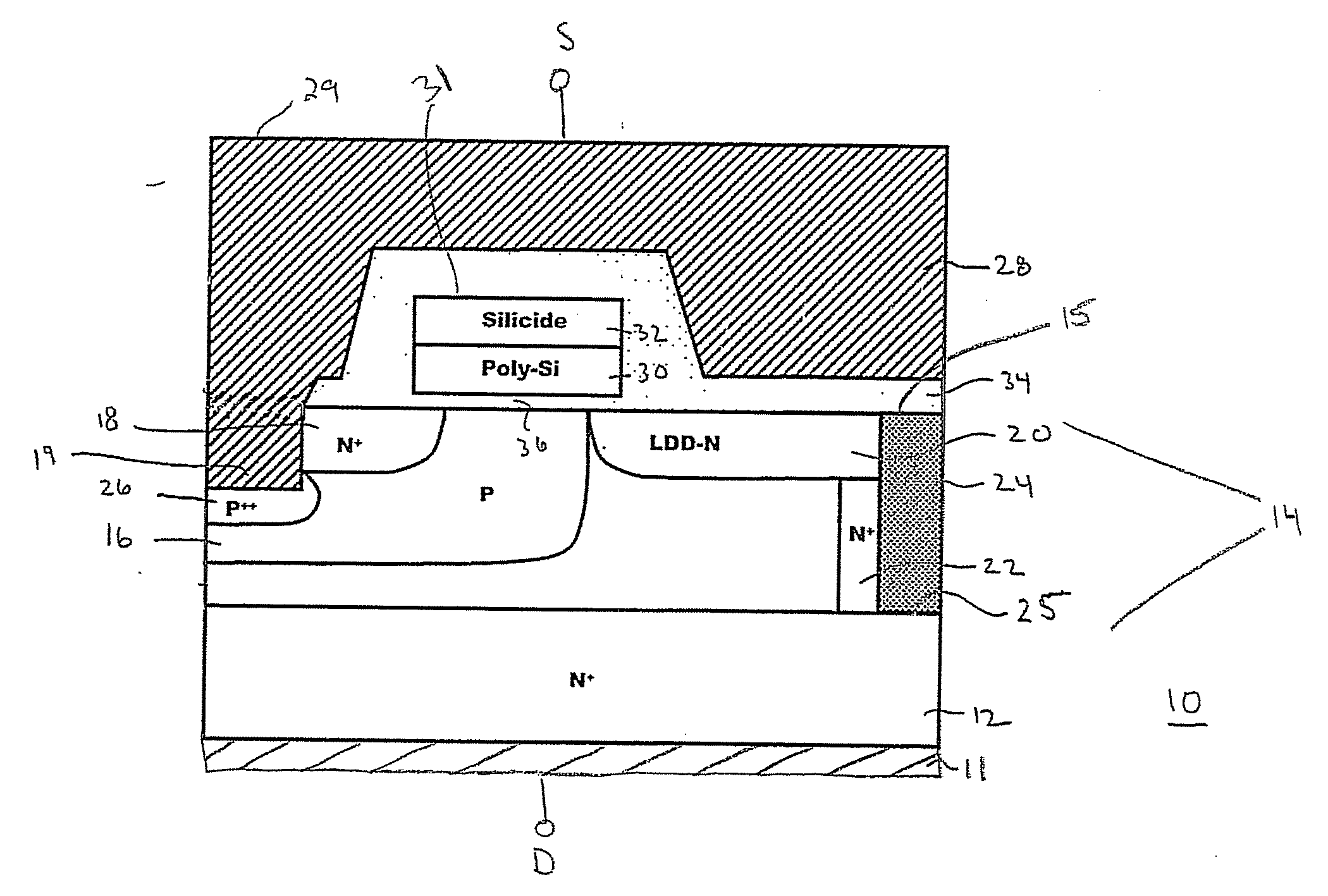
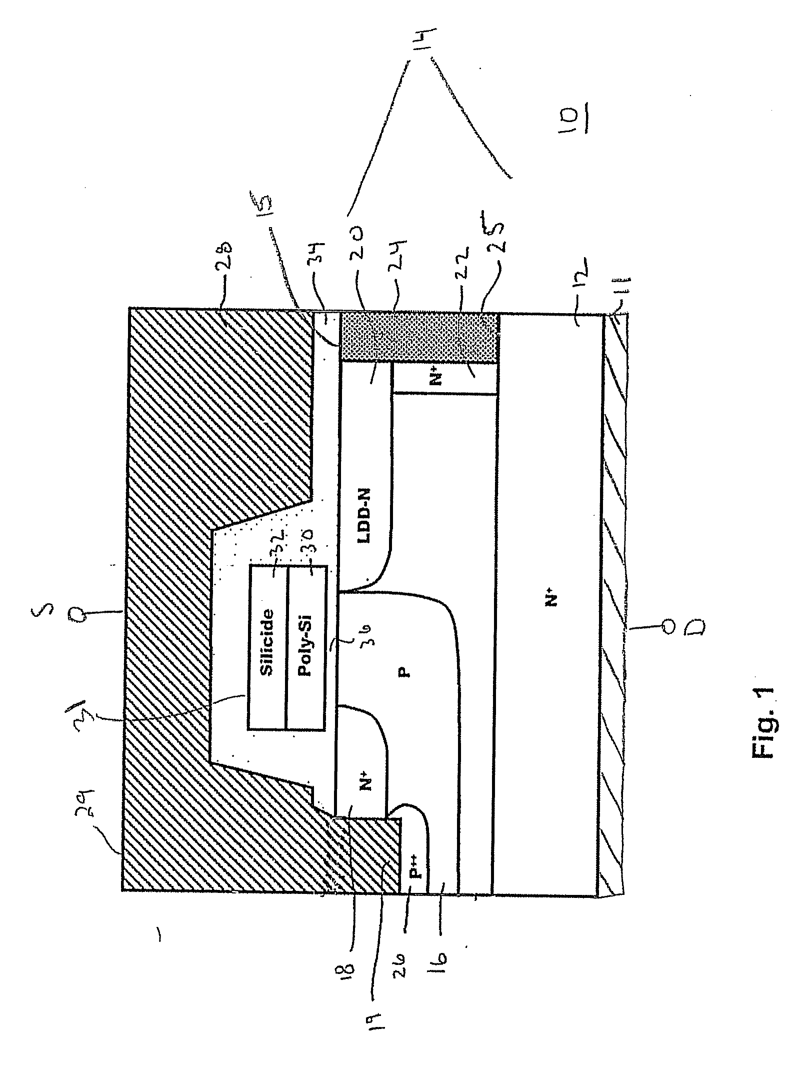
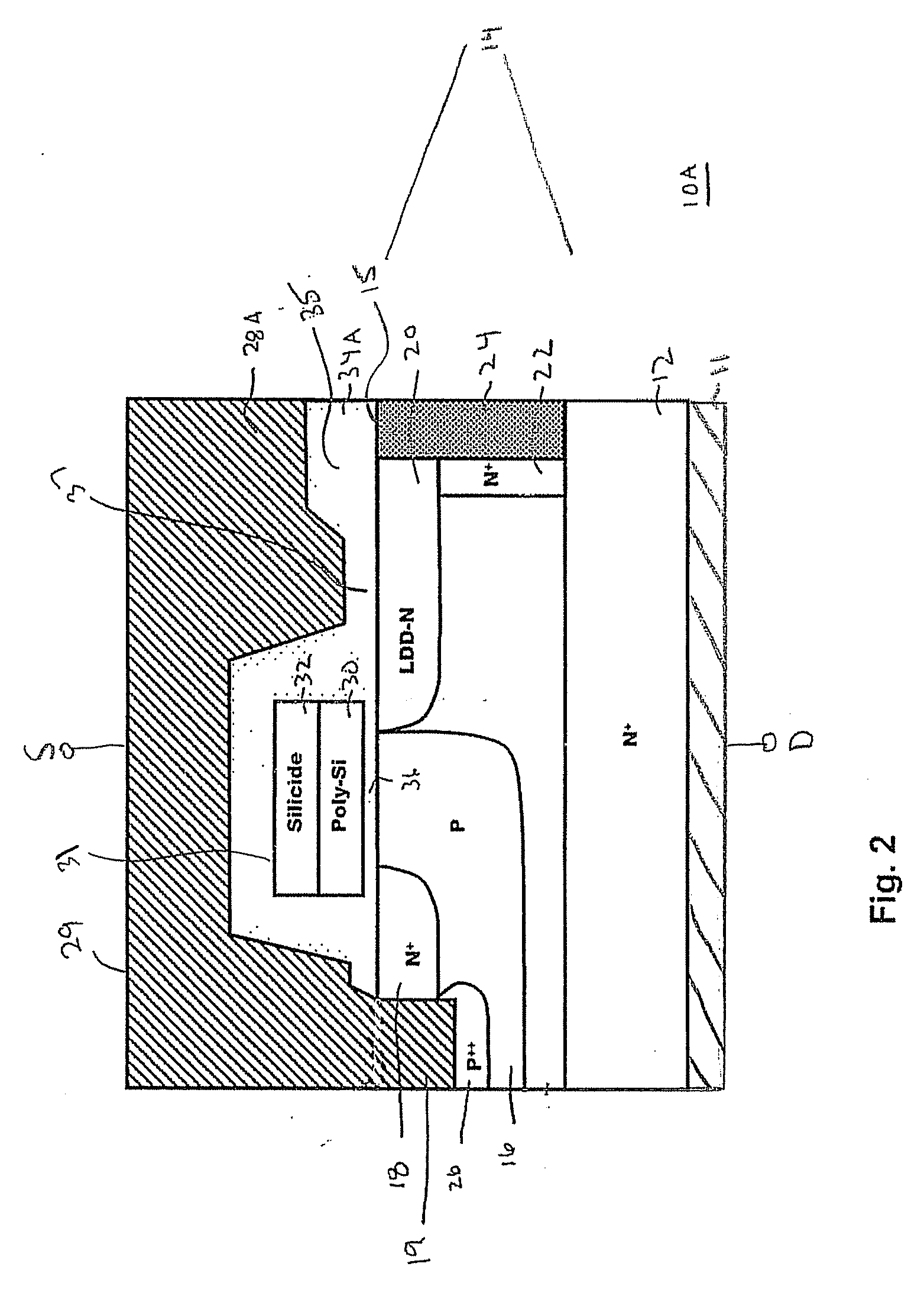
[0022] As used herein, the following dopant concentrations are distinguished using the following notations:

[0023] (a) N++ or P++: dopant concentration of about >5×10¹⁹ atoms / cm3;

[0024] (b) N+ or P+: dopant concentration of about 1×10¹⁸ to 5×10¹⁹ atoms / cm3;

[0025] (c) N or P: dopant concentration of about 5×10¹⁶ to 1×10¹⁸ atoms / cm3;

[0026] (d) N− or P−: dopant concentration of about 1×10¹⁵ to 5×10¹⁶ atoms / cm3; and

[0027] (e) N−− or P−−: dopant concentration of about 15 atoms / cm3.

[0028] In the following description, numerous specific details are set forth, such as material types, doping levels, structural features, processing steps, etc., in order to provide a thorough understanding of the present invention. Those of ordinary skill in the art will understand that the invention described herein may be practiced without many of these details. In other instances, well-known elements, techniques, features, and processing steps have not been described in detail in order to avoid obscuri...


PUM


Abstract

A laterally diffused metal-oxide-semiconductor transistor device includes a substrate having a first conductivity type with a semiconductor layer formed over the substrate. A source region and a drain extension region of the first conductivity type are formed in the semiconductor layer. A body region of a second conductivity type is formed in the semiconductor layer. A conductive gate is formed over a gate dielectric layer that is formed over a channel region. A drain contact electrically connects the drain extension region to the substrate and is laterally spaced from the channel region. The drain contact includes a highly-doped drain contact region formed between the substrate and the drain extension region in the semiconductor layer, wherein a topmost portion of the highly-doped drain contact region is spaced from the upper surface of the semiconductor layer. A source contact electrically connects the source region to the body region.

Description

CROSS-REFERENCE TO RELATED APPLICATION [0001] This application is a continuation-in-part of co-pending U.S. patent application Ser. No. 11 / 180,155 filed Jul. 13, 2005, the entirety of which is hereby incorporated by reference herein.FIELD OF THE INVENTION [0002] The present invention relates to semiconductor structures and more particularly to laterally diffused MOS transistors (LDMOS) and methods of making the same. BACKGROUND OF THE INVENTION [0003] Power MOSFETs (metal oxide semiconductor (MOS) field effect transistors (FET)) are used, for example, as electric switches for high frequency PWM (pulse width modulation) applications such as voltage regulators and / or as load switches in power applications. When used as load switches, where switching times are usually long, cost, size and on-resistance of the switches are the prevailing design considerations. When used in PWM applications, the transistors must exhibit small power loss during switching, which imposes an additional requi...

Claims


Application Information

Patent Timeline
Patent Type & Authority Applications(United States)
IPC IPC(8): H01L29/76H01L21/336
CPCH01L29/0634H01L29/0878H01L29/1095H01L29/402H01L29/41741H01L29/4175H01L29/41758H01L29/41766H01L29/4933H01L29/7802H01L29/7811H01L29/7816H01L29/7823
Inventor KOCON, CHRISTOPHER BOGUSLAWXU, SHUMINGKOREC, JACEK
Owner TEXAS INSTR LEHIGH VALLEY
Why Eureka
Try Eureka