Charge pump circuit and power supply apparatus

a pump circuit and power supply technology, applied in the direction of power conversion systems, dc-dc conversion, instruments, etc., can solve the problems of reducing power conversion efficiency, so as to achieve high efficiency

Inactive Publication Date: 2007-06-21
PANASONIC CORP
View PDF7 Cites 33 Cited by
  • Summary
  • Abstract
  • Description
  • Claims
  • Application Information

AI Technical Summary

Benefits of technology

[0013] It is therefore an object of the present invention to provide a high efficiency charge pump circuit and a power supply apparatus that can sense the output c...

Problems solved by technology

This prior-art charge pump circuit has a disadvantage that the output current level cannot be sensed adequately.
Consequently, power conversion efficiency is greatly reduced without optimal switching operation of a flying capacitor.
For example, when the connection of a flying capacitor is changed based solely on input voltage detection, even when voltage drop is little in the state of light-load current and therefore can be compensated for by means of 2-fold voltage boost operation, the connection may maintain 3-f...

Method used


Image

  • Charge pump circuit and power supply apparatus
  • Charge pump circuit and power supply apparatus
  • Charge pump circuit and power supply apparatus

Examples


embodiment 1

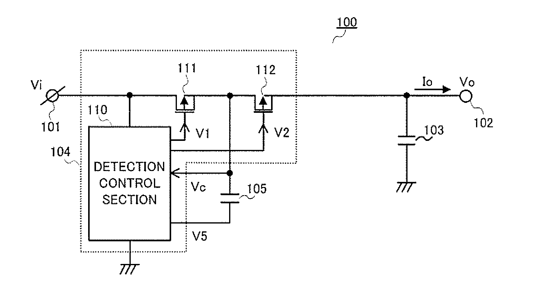
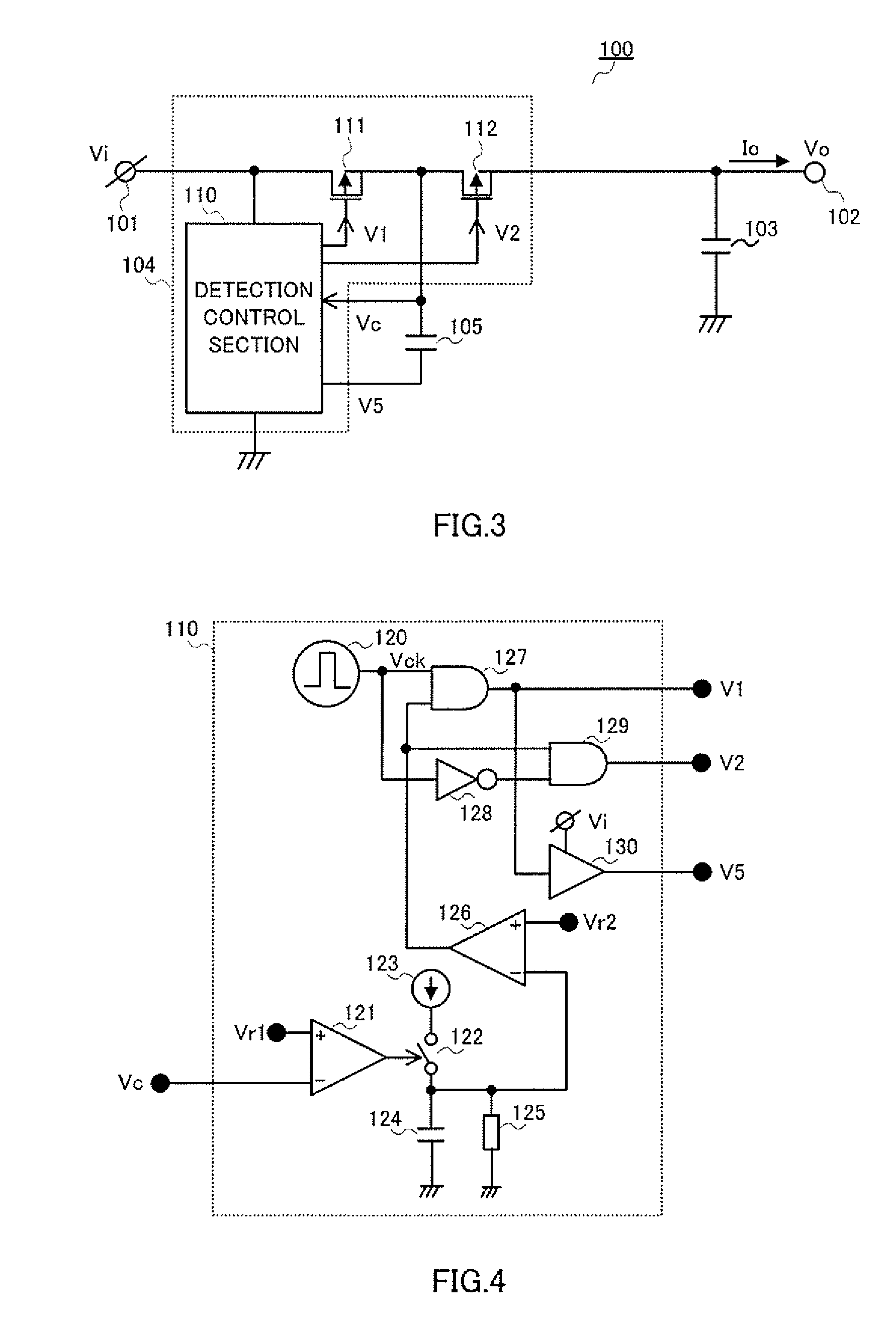
[0045]FIG. 3 is a circuit configuration diagram of a charge pump circuit according to Embodiment 1 of the present invention. This embodiment will describe a case of adopting a charge pump circuit operates in 2-fold voltage boost.

[0046] With reference to FIG. 3, charge pump circuit 100 comprises: input terminal 101, to which an input voltage Vi is applied; output terminal 102, which outputs an output voltage Vo and an output current Io; output capacitor 103, which is connected between output terminal 102 and the ground to smooth the output of charge pump circuit 100; detection control section 110, which detects the voltage of flying capacitor 105 and senses the output current from output terminal 102; switching circuit 104, which is formed with switch element 111 and switch element 112 of PMOS transistors; and flying capacitor 105, one end of which is connected to a connection point between switch element 111 and switch element 112 and the other end of which is applied a drive signa...

embodiment 2

[0072] A charge pump circuit and current detection function for 2-fold voltage boost operation were described with Embodiment 1, and, in addition, an over-current protection circuit was described as an example of that current detection function.

[0073] With this embodiment, a charge pump circuit and current detection function for 1.5-fold voltage boost operation will be described, and, in addition, switch between 1.5-fold voltage boost operation and 1.0-fold voltage boost operation will be described as an example of that current detection function. FIG. 6 is a circuit configuration diagram of a charge pump circuit according to Embodiment 2 of the present invention. With reference to FIG. 4, for a description of this embodiment, the same numbers are assigned to the same parts as in FIG. 3.

[0074] With reference to FIG. 6, charge pump circuit 200 comprises: input terminal 101 to which an input voltage Vi is applied; output terminal 102 which outputs an output voltage Vo and an output ...

embodiment 3

[0097] Switch between 1.5-fold voltage boost operation and 1.0-fold voltage boost operation was described with Embodiment 2 as an example of applying a current detection function to a charge pump circuit for 1.5-fold voltage boost operation. In this embodiment, switch between 2-fold voltage boost and 3-fold voltage boost with an addition of a voltage stabilizing function will be described.

[0098]FIG. 10 is a circuit configuration diagram of a charge pump circuit according to Embodiment 3 of the present invention. With reference to FIG. 8, for a description of this embodiment, the same numbers are assigned to the same units as shown in FIG. 6.

[0099] With reference to FIG. 10, charge pump circuit 300 comprises: input terminal 101 to which an input voltage Vi is applied; output terminal 102 which outputs an output voltage Vo and an output current Io; output capacitor 103 which is connected between output terminal 102 and the ground, and smoothes the output of charge pump circuit 300; ...


PUM


Abstract

A high efficiency charge pump circuit and a power supply apparatus that can sense the output current level and change the connection of flying capacitors. The charge pump circuit includes a switching circuit that performs a switching operation of alternately switching between the charge state of charging flying capacitor from input terminal and a discharge state of discharging flying capacitor to output terminal. A flying capacitor, one end of which is connected to a connection point between two switch elements and to the other end of which a drive signal from switching circuit is applied. A detection control section detects a voltage of flying capacitor and outputs various drive signals. The charge pump circuit detects the voltage of the flying capacitor and senses the output current that is output from output terminal according to a relationship indicating the difference between the input voltage and the initial value Vc0 of the detected voltage of flying capacitor in the charge state.

Description

BACKGROUND OF THE INVENTION [0001] 1. Field of the Invention [0002] The present invention relates to a charge pump circuit and power supply apparatus for supplying a stable voltage to various types of electronic devices. [0003] 2. Description of the Related Art [0004] Recently, electronic devices having batteries, such as mobile devices, require more than the battery voltage for display devices. Among these devices, charge pump circuits are widely used as DC-DC converters that do not use inductors, to address the need for further reduction of power consumption. The voltage converting circuit disclosed in Patent Document 1 (Japanese Patent Application Laid-Open No. 2001-218451) is an example of a prior-art charge pump circuit. [0005]FIG. 1 is a circuit diagram for the charge pump circuit disclosed in Patent Document 1. FIG. 2 is an operation waveform chart of the charge pump circuit as shown in FIG. 1. [0006] With reference to FIG. 1, “1” designates an input terminal where an input v...

Claims


Application Information

Patent Timeline
IPC IPC(8): H02M3/18
CPCH02M3/07
Inventor UENO, TOMOTAKAISHII, TAKUYA
Owner PANASONIC CORP
Why Eureka
Try Eureka