Flash memory device and method for manufacturing the same

a flash memory and memory technology, applied in the direction of semiconductor devices, electrical devices, transistors, etc., can solve the problems of data storage and retention capacity degrade, and achieve the effect of degrading layer quality and degrading data storage ability

Inactive Publication Date: 2007-06-28
SK HYNIX INC
View PDF9 Cites 3 Cited by
  • Summary
  • Abstract
  • Description
  • Claims
  • Application Information

AI Technical Summary

Benefits of technology

[0005]One embodiment provides a flash memory device and a method of manufacturing the same, wherein degradation of the layer quality of a tunnel oxide

Problems solved by technology

Accordingly, a problem arises because the data

Method used


Image

  • Flash memory device and method for manufacturing the same
  • Flash memory device and method for manufacturing the same
  • Flash memory device and method for manufacturing the same

Examples


Embodiment Construction

[0023]The invention is described in detail in connection with certain exemplary embodiments with reference to the accompanying drawings.

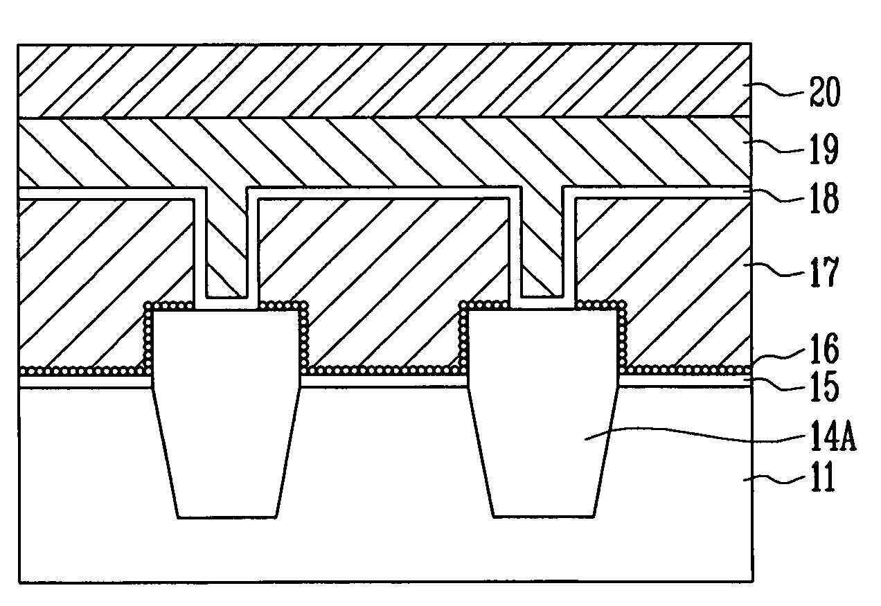
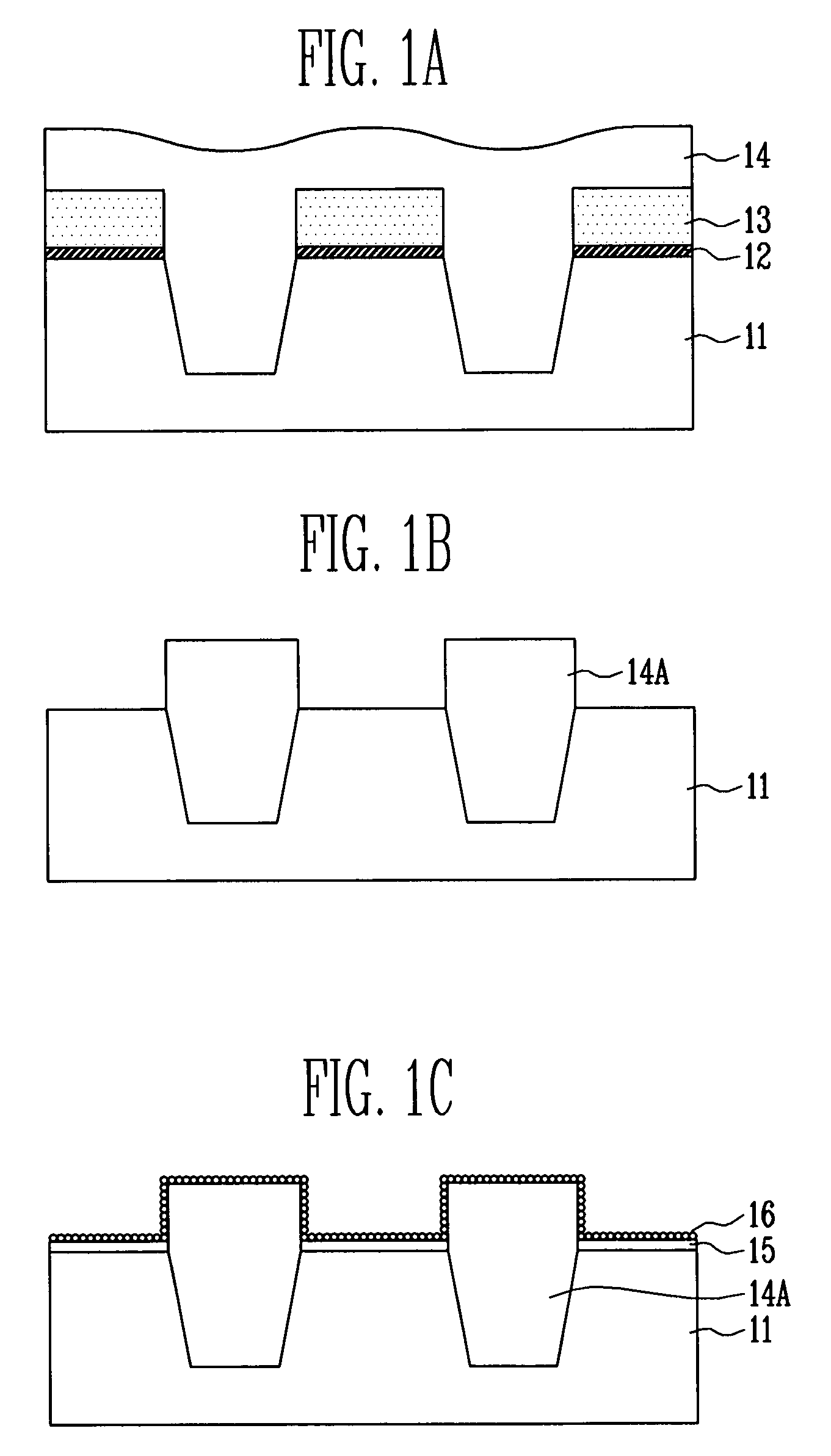
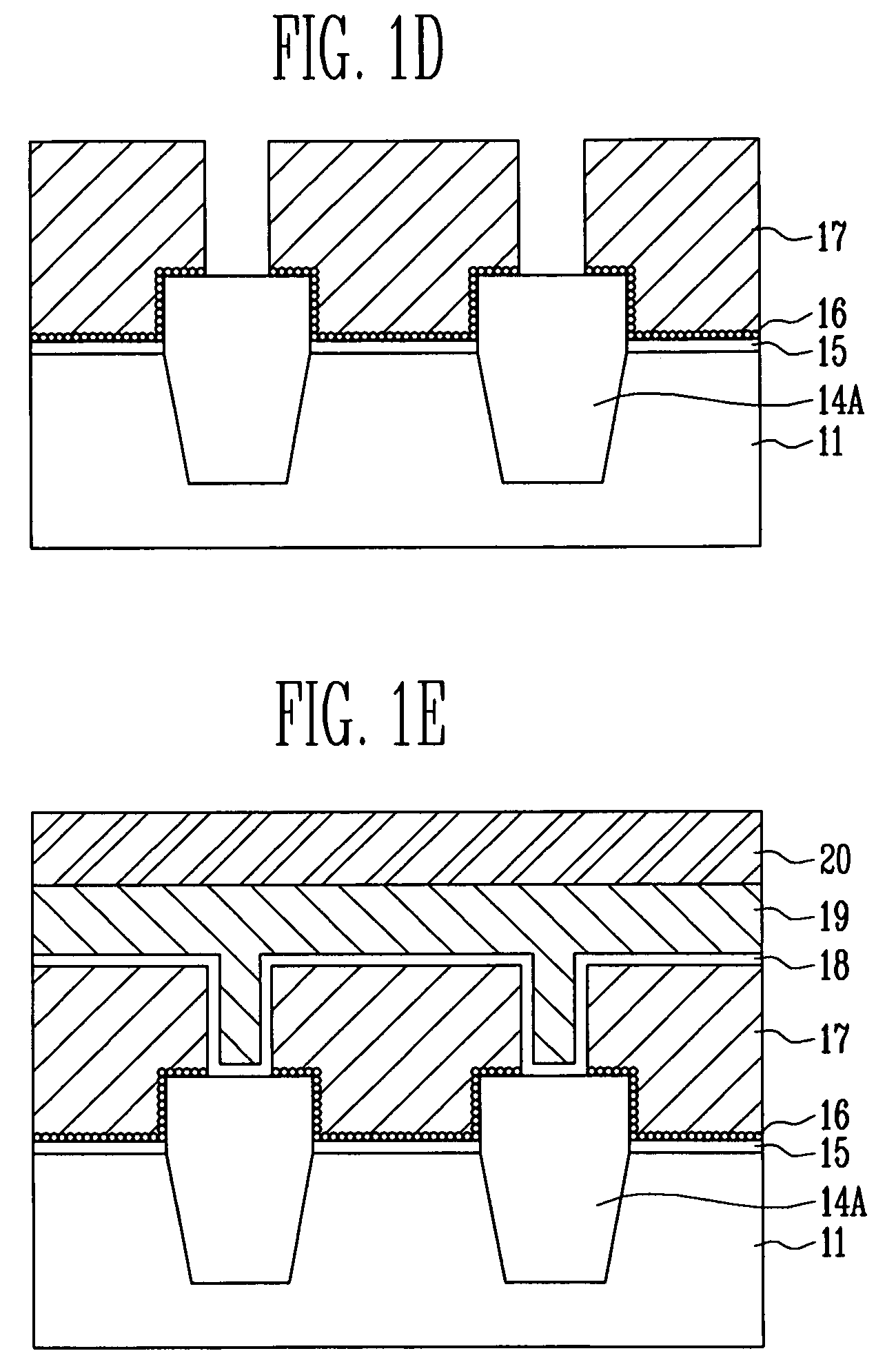
[0024]FIGS. 1A to 1E are cross-sectional views illustrating a method of manufacturing a flash memory device according to an embodiment of the invention.

[0025]Referring to FIG. 1A, a pad oxide layer 12 and a pad nitride layer 13 are sequentially formed on a semiconductor substrate 11. Predetermined regions of the pad nitride layer 13 and the pad oxide layer 12 are etched by photolithography and etch processes using an isolation mask. The semiconductor substrate 11 is then etched at a predetermined depth, forming trenches. An oxide layer 14 is formed on the entire structure so that the trench is buried.

[0026]Referring to FIG. 1B, the oxide layer 14 is polished so that the pad nitride layer 13 is exposed. The pad nitride layer 13 and the pad oxide layer 12 are then stripped. Accordingly, isolation structures 14A defining an active region and a field re...


PUM


Abstract

A flash memory device and a method of manufacturing the same, wherein a silicon layer having a micro grain is formed between a tunnel oxide layer and a floating gate using a hemi-spherical grain (HSG) method, thereby preventing the dopant of the floating gate from being diffused into the tunnel oxide layer. According to one embodiment, the flash memory device includes isolation structures formed in predetermined regions of a semiconductor substrate, for defining an active region and a field region, a tunnel oxide layer formed on the semiconductor substrate of the active region, and a floating gate formed in a predetermined region on the active region to overlap with a part of the isolation structure, an underlying given portion and the remaining portions of the floating gate having different grain sizes.

Description

BACKGROUND OF THE INVENTION[0001]The invention relates generally to a flash memory device and a method of manufacturing the same. More particularly, the invention relates to a flash memory device and a method of manufacturing the same, in which a silicon layer having a micro grain is formed between a tunnel oxide layer and a floating gate using a hemi-spherical grain (HSG) method, thereby preventing the dopant of the floating gate from being diffused into the tunnel oxide layer.[0002]A memory device, e.g. a NAND flash memory device, includes a plurality of cell blocks. One cell block includes a plurality of cell strings in which a plurality of cells for storing data are in series connected to form one string, and a drain select transistor and a source select transistor formed between the cell string and the drain, and the cell string and the source, respectively. An exemplary method of fabricating the NAND flash memory cell is described below.[0003]A buffer oxide layer and a pad nit...

Claims


Application Information

Patent Timeline
IPC IPC(8): H01L29/788
CPCH10B69/00H10B41/30H01L29/40114H01L21/28185
Inventor YANG, YOUNG HO
Owner SK HYNIX INC
Why Eureka
Try Eureka