Electroluminescent display brightness level adjustment

a technology of electroluminescent display and brightness level, applied in the direction of instruments, static indicating devices, etc., can solve the problems of power consumption dependent upon input signal, power consumption dependent on display device power, power consumption dependent on emissive display technology, etc., to reduce apparent artifacts, large and/or bright displays, and high current levels

Active Publication Date: 2007-06-28
GLOBAL OLED TECH
View PDF14 Cites 56 Cited by
  • Summary
  • Abstract
  • Description
  • Claims
  • Application Information

AI Technical Summary

Benefits of technology

[0012] In accordance with various embodiments, the present invention provides a system and method that reduces apparent artifacts in an electroluminescent display such as an OLED display that can result when driving the display such as to require high current levels along power lines with a finite resistance in order to enable the manufacture of larger and / or brighter displays. The invention may additionally reduce the overall power consumed by the display, as well as reduce the heat that is generated within the display. Alternately, the invention may increase the luminance of the display device without creating the artifacts that would typically be present. Further, the invention preferably additionally provides these advantages on a display having more than three-color channels.

Problems solved by technology

The power consumption of emissive display technologies, however, is directly dependent upon the signal that is input to the display device since the typical emissive display will require almost no power to produce a black image but a significantly higher power to produce a highly luminous white image.
Like CRTs and plasma displays, devices constructed based on OLEDs are emissive and have the characteristic that power consumption is dependent upon the input signal.
However, these disclosures do not address the fact that active matrix electroluminescent displays such as OLED displays use a driving arrangement that is significantly different in structure than is applied in plasma displays and therefore require a different approach to power reduction to avoid imaging artifacts while reducing the power of the display device.
However, current is typically provided to a large number of OLEDs by a single pair of power lines.
This results in variation in the voltage supplied to each pixel driving circuit along the power lines, and subsequent variation in both the current and luminance of each OLED supplied by the power lines.
Further, because the resistance of the power lines increases with length, this IR drop will result in the gradual loss of luminance for OLEDs along the power lines as the distance from the power source increases.
This loss of luminance has the potential to create undesirable imaging artifacts.
IR drop may also occur in electroluminescent display devices which employ other active matrix drive schemes and can result in undesirable imaging artifacts when using these drive schemes as well.
In some cases, a highly conductive plane of material can be used in place of one or more individual power lines to reduce the resistance, but this depends on the structure of the device, and it is not always possible to find materials with sufficient properties and / or methods to produce this plane of material.
Similarly, the materials that are available to reduce resistance and the cross-sectional area of individual power lines are often fixed by the manufacturing technology that is available, so it is often not cost effective to reduce the resistance of the power lines.
This often limits the size or luminance of displays that can be produced using OLED technology.
While this technique does reduce the peak currents that must be delivered and therefore limits the voltage drop that can occur across the power lines due to IR drop, this technique does not allow a predictable response at each OLED.
In fact, it can actually result in additional undesirable artifacts as some TFTs in the panel may be driven at a voltage level below their saturation region, resulting in a further reduction, and more variability, in the current conducted through the OLEDs for a given data voltage.
For this reason, the technique taught, while controlling the power of an active matrix OLED display, can contribute to unintended luminance non-uniformities in the display device, reducing the quality of the image that is displayed.
This approach does not, however, solve the problems associated with the earlier disclosure and does not provide a method for adjusting the contrast in response to changes in display luminance.
However, the described methods can still result in objectionable artifact levels as this disclosure does not recognize or propose a solution to the problem that IR drop can be different for different power lines and that different luminance levels may result between light emitting elements driven by neighboring power lines when high current loads are present.

Method used


Image

  • Electroluminescent display brightness level adjustment
  • Electroluminescent display brightness level adjustment
  • Electroluminescent display brightness level adjustment

Examples


Embodiment Construction

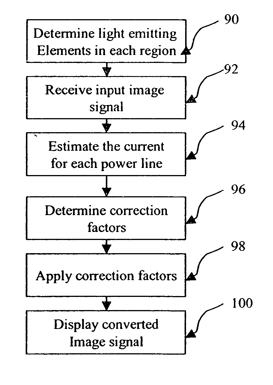
[0023] The present invention provides a display system including a display driver that analyzes the input signal to an electroluminescent display and modifies this signal to limit the maximum unintended difference in current draw among regions of the display where the regions represent groups of light-emitting elements, such as OLEDs, that are driven by neighboring pairs of power lines.

[0024] More specifically an electroluminescent display system is provided, comprising: a display composed of an array of regions, wherein the current to each of the regions is provided by a pair of power lines and wherein each region includes an array of light emitting elements for emitting light; a pixel driving circuit for independently controlling the current to each light-emitting element in response to an image signal, wherein the intensity of the light output by each light emitting element is dependent upon the current provided to the light emitting element; and a display driver for receiving a...


PUM


Abstract

An electroluminescent display system, comprising: a) a display composed of an array of regions, wherein the current to each of the regions is provided by a pair of power lines and wherein each region includes an array of light emitting elements for emitting light; b) a pixel driving circuit for independently controlling the current to each light-emitting element in response to an image signal, wherein the intensity of the light output by the light emitting elements is dependent upon the current provided to each light emitting element; and c) a display driver for receiving an input image signal and generating a converted image signal for driving the light emitting elements in the display, wherein the display driver analyzes the input image signal to estimate the current that would result at, at least, one point along at least one of the power lines providing current to each of the regions, if employed without further modification, based upon device architecture and material and performance characteristics of device components, and generates the converted image signal as a function of the input image signal and the estimated currents.

Description

FIELD OF THE INVENTION [0001] The present invention relates to electroluminescent display systems and a method for automatically adjusting the behavior of an electroluminescent display dependent upon input image information. BACKGROUND OF THE INVENTION [0002] Emissive display technologies, including displays based on cathode-ray tubes (CRTs) and plasma excitation of phosphors have become very popular within many applications. This is typically due to the fact that these technologies natively have superior performance characteristics over reflective or transmissive display technologies, such as displays produced using liquid crystals (LCDs). Among the superior characteristics of these displays is higher dynamic range, wider viewing angle, and, often, lower power consumption. The power consumption of emissive display technologies, however, is directly dependent upon the signal that is input to the display device since the typical emissive display will require almost no power to produc...

Claims


Application Information

Patent Timeline
Patent Type & Authority Applications(United States)
IPC IPC(8): G09G3/30
CPCG09G3/3233G09G2300/0426G09G2300/0842G09G2320/0223G09G2320/0233
Inventor MILLER, MICHAEL E.MURDOCH, MICHAEL J.LUDWICKI, JOHN E.
Owner GLOBAL OLED TECH
Why Eureka
Try Eureka