Electro-optical device, manufacturing method thereof, and electronic apparatus

a technology of electro-optical devices and manufacturing methods, applied in non-linear optics, instruments, optics, etc., can solve the problems of deterioration of picture quality due to display spots, deterioration of humidity resistance of liquid crystal display devices, etc., to prevent the alignment layer from being peeled, improve the adhesion between the alignment layer and the lower layer, and improve the humidity resistance of electro-optical devices

Inactive Publication Date: 2007-06-28
138 EAST LCD ADVANCEMENTS LTD
View PDF13 Cites 52 Cited by
  • Summary
  • Abstract
  • Description
  • Claims
  • Application Information

AI Technical Summary

Benefits of technology

[0016] An advantage of some aspects of the invention is to provide an electro-optical device, which is capable of improving adhesion between an alignment layer and a layer formed below the alignment in order to prevent humidity from penetrating into an effective pixel region, thereby improving humidity resistance of the electro-optical device while preventing the alignment layer from being peeled from the layer formed below the alignment when the alignment layer is subjected to a rubbing treatment, a manufacturing method thereof, and an electronic apparatus having the electro-optical device. Another advantage of the invention is to provide an electro-optical device, which is capable of improving transmittance while maintaining humidity resistance, thereby making it possible to attain higher quality of picture, a manufacturing method thereof, and an electronic apparatus having the electro-optical device.
[0017] According to an aspect of the invention, there is provided an electro-optical device including a first substrate, a second substrate facing the first substrate, with a sealing material interposed between the first and second substrates, liquid crystals being interposed in at least an effective pixel region between the first and second substrates, including: an alignment layer that is formed on at least one of the first and second substrates immediately below the sealing material and aligns the liquid crystals; and a lower layer formed below the alignment layer. A transparent conductive layer that is firmly adhered to the alignment layer and the lower layer is formed in a region covering at least the sealing material between the alignment layer and the lower layer.
[0018] With this configuration, even when the electro-optical device is used under high humidity conditions, humidity can be prevented from penetrating from the outside of the device into a region defined by the sealing material of at least one of the first and second substrates through a gap between the alignment layer and the lower layer formed below the alignment layer. As a result, humidity resistance of the electro-optical device is improved. In addition, as the adhesion between the alignment layer and the lower layer is improved, the alignment layer can be prevented from being peeled from the lower layer.
[0019] An external connection terminal may be formed on at least one of the first and second substrates, and an electrode is formed in the effective pixel region, and the transparent conductive layer is formed on the entire surface of a region except the external connection terminal and the electrode between the alignment layer and the lower layer.
[0020] With this configuration, since the transparent conductive layer does not contact the external connection terminal and the electrode of the effective pixel region, there does not occur a circuit-short between external connection terminals or between electrodes. In addition, even when the device is used under high humidity conditions, humidity can be prevented from penetrating from the outside of the device into a region defined by the sealing material of at least one of the first and second substrates through a gap between the alignment layer and the lower layer formed below the alignment layer. As a result, humidity resistance of the electro-optical device is improved. In addition, as the adhesion between the alignment layer and the lower layer is improved, the alignment layer can be prevented from being peeled from the lower layer.
[0021] A groove may be formed in the region covering at least the sealing material at a surface of the lower layer that contacts the transparent conductive layer.

Problems solved by technology

However, since the alignment layer formed of polyimide does not adhere well to the insulating layer formed of the above-mentioned material, humidity penetrates into the effective pixel region through a gap between the insulating layer and the alignment layer while the assembled liquid crystal display device is used under high humidity conditions, which results in deterioration of the humidity resistance of the liquid crystal display device and hence deterioration of picture quality due to display spots.
The above problems are not limited to the insulating layer and also arise due to poor adhesion between the alignment layer and a layer formed below the alignment layer.
However, the liquid crystal display device disclosed in Patent Document 1 does not consider the above problems.
However, the technique disclosed in Patent Document 2 also has a problem of deterioration of humidity resistance of the liquid crystal display device due to poor surface adhesion between the optical thin films formed of nitride films or the like and the alignment layer made of polyimide or the like.
In addition, since the seal low-side layer is formed in the pixel electrode forming process, complexity of the manufacturing process is not caused at all.

Method used


Image

  • Electro-optical device, manufacturing method thereof, and electronic apparatus
  • Electro-optical device, manufacturing method thereof, and electronic apparatus
  • Electro-optical device, manufacturing method thereof, and electronic apparatus

Examples


first embodiment

[0111] First, a first embodiment of the invention will be described.

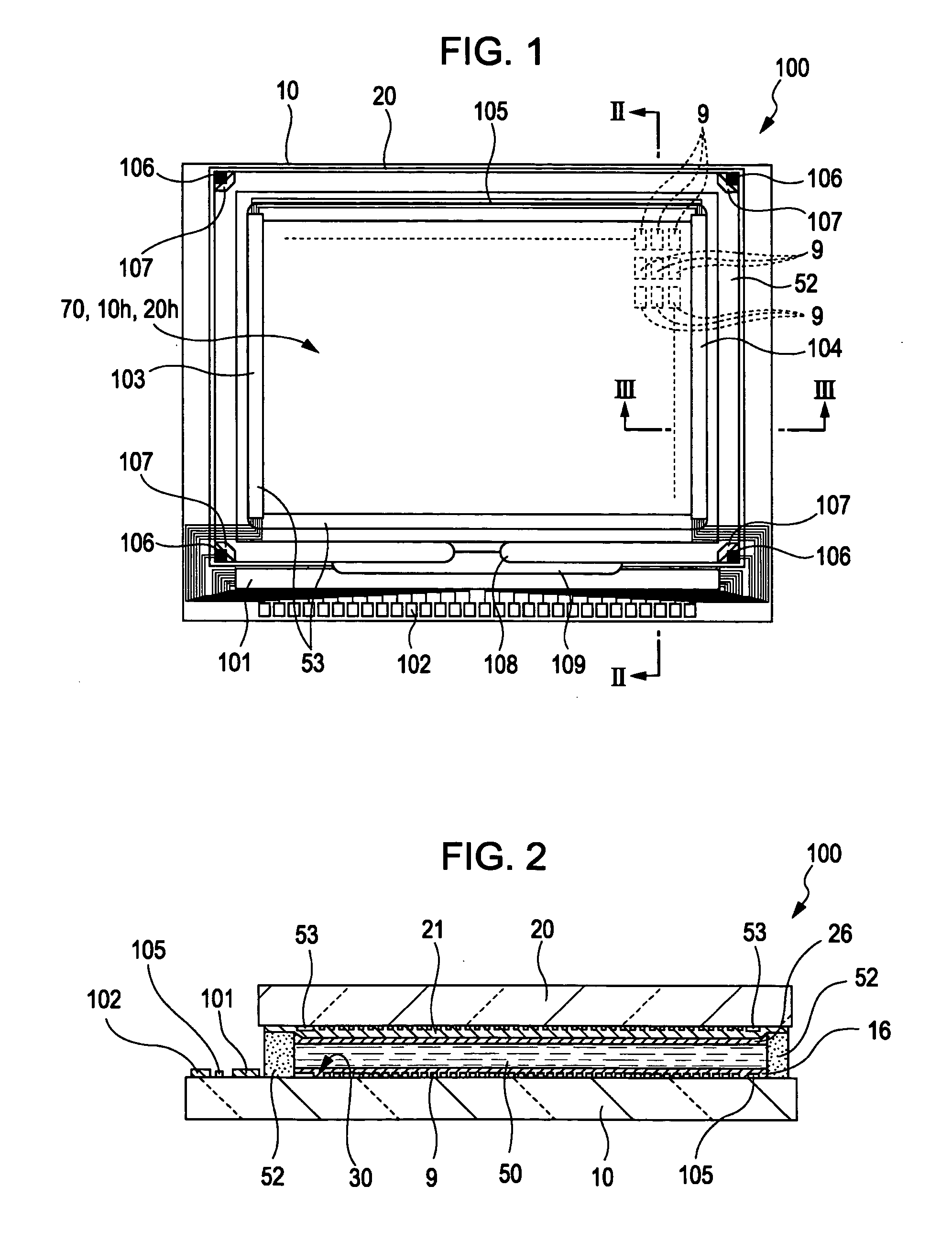
[0112]FIG. 1 is a plan view of a liquid crystal display device according to a first embodiment, and FIG. 2 is a sectional view taken along line II-II of FIG. 1.

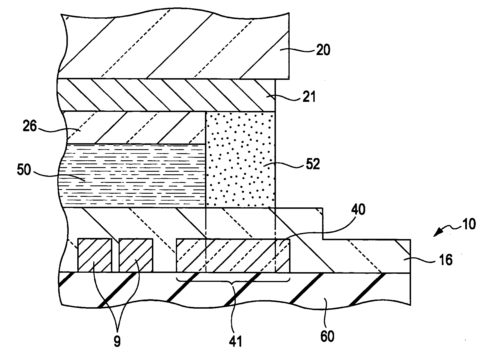
[0113] As shown in FIGS. 1 and 2, a liquid crystal display device 100 includes a TFT substrate 10, as a first substrate, which is formed of, for example, a quartz substrate, a glass substrate or a silicon substrate, an opposite substrate 20, as a second substrate, which faces the TFT substrate 10 and is formed of, for example, a glass substrate or a quartz substrate, and a liquid crystal layer 50 which is constituted by an electro-optical material and is interposed between the TFT substrate 10 and the opposite substrate 20. The TFT substrate 10 and the opposite substrate 20 are bonded together by a sealing material 52.

[0114] A display region 10h of the TFT substrate 10, which constitutes an effective pixel region (hereinafter, referred to as a display regi...

second embodiment

[0149] Next, a second embodiment of the invention will be described.

[0150]FIG. 8 is a front view showing a schematic configuration of a TFT substrate of a liquid crystal display device according to a second embodiment of the invention, and FIG. 9 is a partial sectional view taken along line IX-IX of FIG. 8.

[0151] A liquid crystal display device according to the second embodiment is different from the liquid crystal display device 100 of the first embodiment as shown in FIGS. 1 to 7 in that the former has a configuration that the alignment layer 16 is firmly adhered to the insulating layer 60 without using the transparent conductive layer 40. Therefore, in the second embodiment, only this difference will be described, and the same elements as the first embodiment are denoted by the same reference numerals, explanation of which will be omitted.

[0152] In FIGS. 8 and 9, the light shield film 53, the data line driving circuit 101, the external connection terminals 102, the scan line d...

third embodiment

[0170] Next, a third embodiment of the invention will be described.

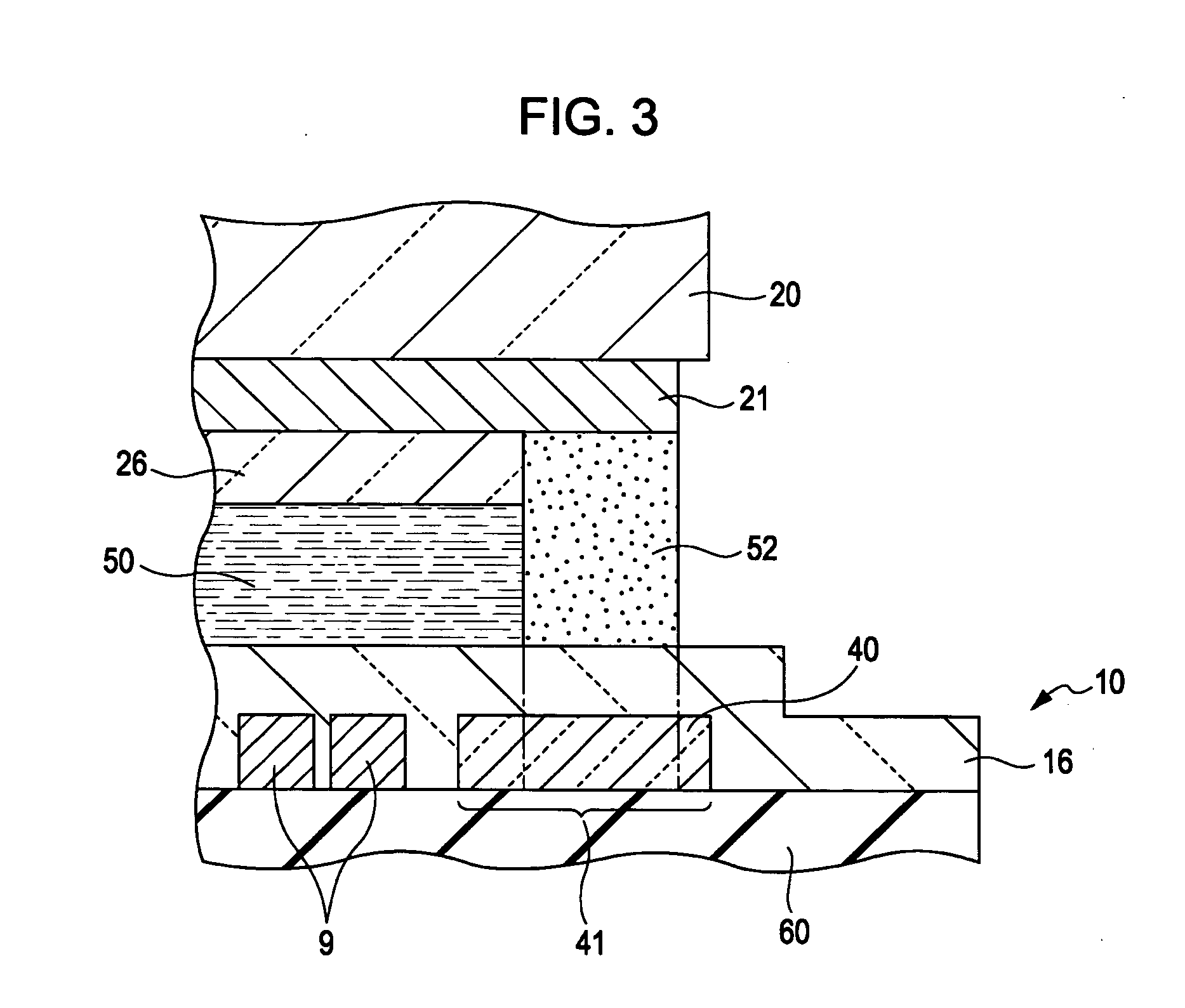
[0171]FIG. 16 is a partial sectional view of a TFT substrate of a liquid crystal display device according to a third embodiment of the invention. A liquid crystal display device according to the third embodiment is different from the liquid crystal display device of the first embodiment as shown in FIGS. 1 to 7 and the liquid crystal display device of the second embodiment as shown in FIGS. 8 and 9 in that the former has a configuration that the alignment layer 16 is firmly adhered to the insulating layer 60 using a transparent conductive layer and a concave groove. Therefore, in the third embodiment, only this difference will be described, and the same elements as the first and second embodiments are denoted by the same reference numerals, explanation of which will be omitted.

[0172] As shown in FIG. 16, the transparent conductive layer 40 is formed on a surface 60t of the insulating layer 60 of a TFT substrate 310...


PUM

PropertyMeasurementUnit
refractive indexaaaaaaaaaa

Abstract

An electro-optical device including a first substrate, a second substrate facing the first substrate, with a sealing material interposed between the first and second substrates, liquid crystals being interposed in at least an effective pixel region between the first and second substrates, comprises an alignment layer that is formed on at least one of the first and second substrates immediately below the sealing material and aligns the liquid crystals, and a lower layer formed below the alignment layer, wherein a transparent conductive layer that is firmly adhered to the alignment layer and the lower layer is formed in a region covering at least the sealing material between the alignment layer and the lower layer.

Description

BACKGROUND [0001] 1. Technical Field [0002] The present invention relates to an electro-optical device such as a liquid crystal display device including, for example, a first substrate, a second substrate facing the first substrate, with a sealing material interposed between the first and second substrates, and a liquid crystal layer placed in at least an effective pixel region between the first and second substrates, a manufacturing method thereof, and an electronic apparatus such as a liquid crystal projector having the electro-optical device. [0003] 2. Related Art [0004] As widely known in the art, as one example of electro-optical devices, a liquid crystal display device has a structure where a liquid crystal layer is interposed between two substrates, each substrate being formed of a glass substrate, a quartz substrate or the like, a plurality of switching elements, such as thin-film transistors (TFTs), and a plurality of pixel electrodes are arranged in the form of a matrix on...

Claims


Application Information

Patent Timeline
Patent Type & Authority Applications(United States)
IPC IPC(8): G02F1/1337G02F1/1339
CPCG02F1/1337G02F1/1339G02F2202/28
Inventor YOKOKAWA, MAGOYUKINAKAMURA, TEIICHIRO
Owner 138 EAST LCD ADVANCEMENTS LTD
Why Eureka
Try Eureka