Eureka AIR delivers breakthrough ideas for toughest innovation challenges, trusted by R&D personnel around the world.

Gate induced drain leakage current reduction by voltage regulation of master wordline

Inactive Publication Date: 2007-06-28
POLARIS INNOVATIONS
View PDF8 Cites 12 Cited by
  • Summary
  • Abstract
  • Description
  • Claims
  • Application Information

AI Technical Summary

Benefits of technology

[0005] Briefly, a semiconductor integrated circuit device and method are provided for reducing gate induced leakage current associated with circuits of the semiconductor electrical device, such as a semiconductor integrated circuit memory device. During a standby mode, a voltage supplied to a plurality of circuits is reduced so as to reduce gate induced leakage (GIDL) current associated with said plurality of circuits. During time intervals while in the standby mode, the voltage supplied to a subset of said plurality of c

Problems solved by technology

Thus, a tension exists between designing the smallest possible semiconductor device but still maximizing the power consumption efficiency of the semiconductor device.
Nevertheless, only recently has the feature size of semiconductor process technologies become so small that reducing the GIDL current has become a design issue.

Method used


Image

  • Gate induced drain leakage current reduction by voltage regulation of master wordline
  • Gate induced drain leakage current reduction by voltage regulation of master wordline
  • Gate induced drain leakage current reduction by voltage regulation of master wordline

Examples


Embodiment Construction

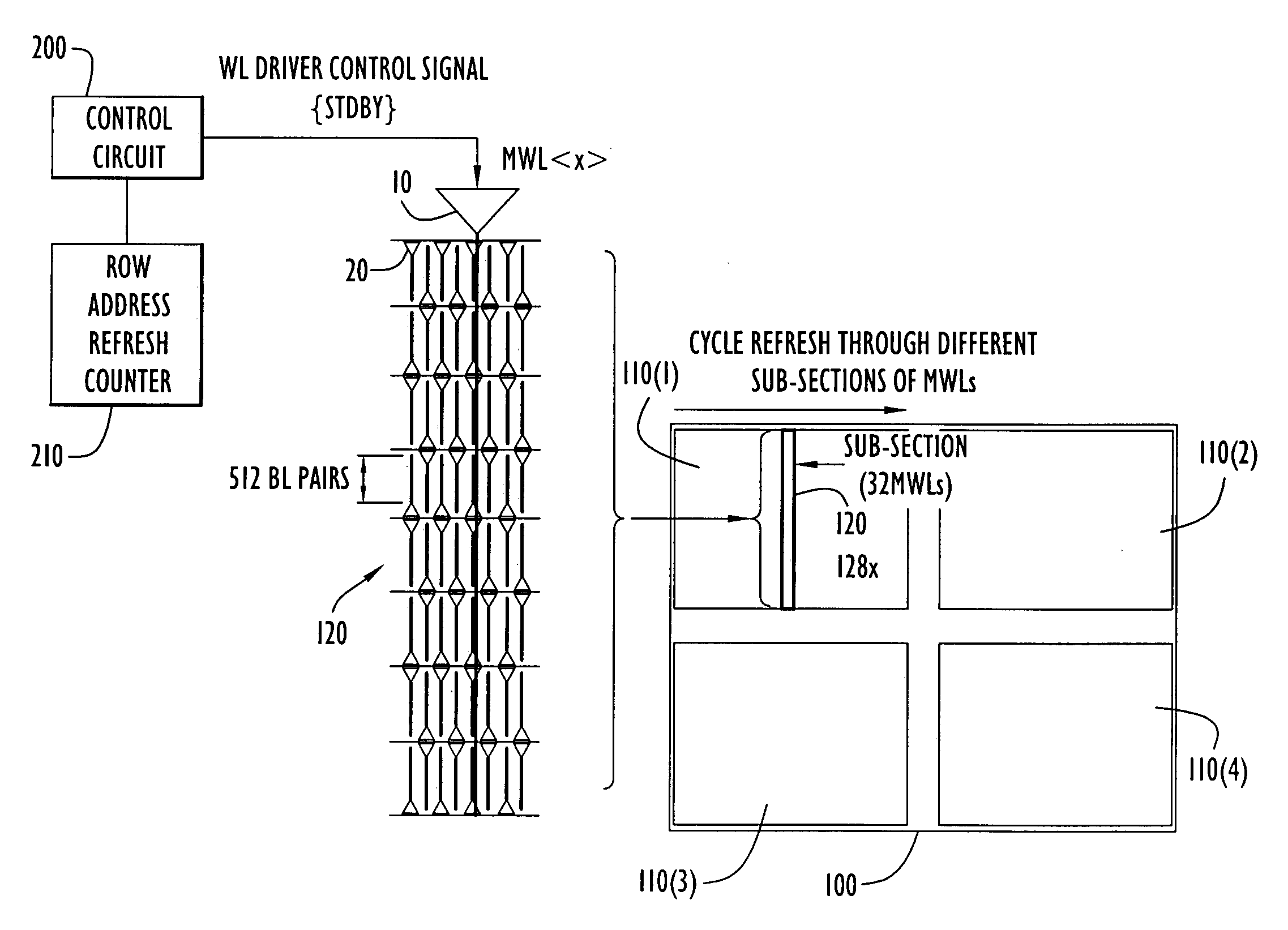
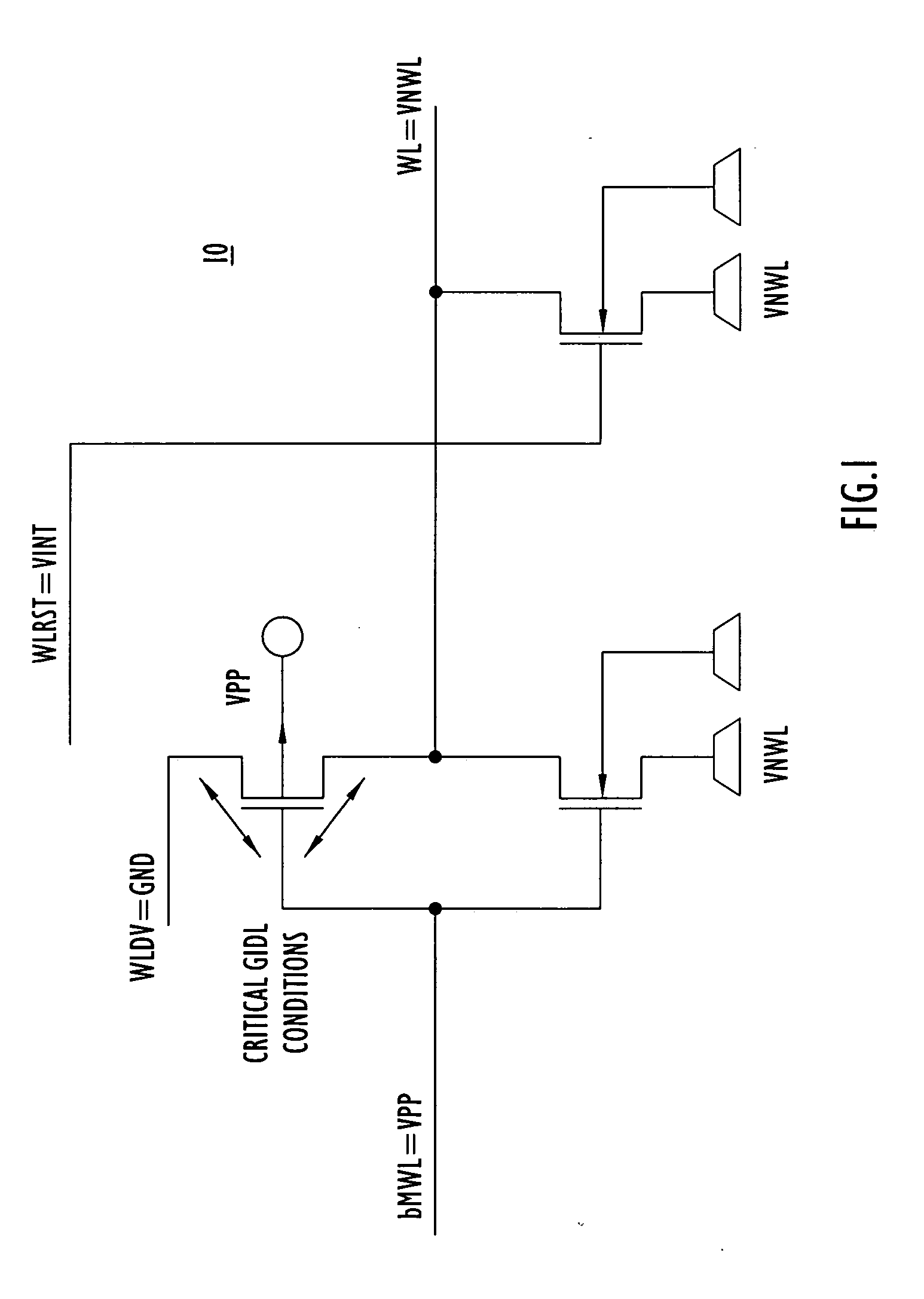
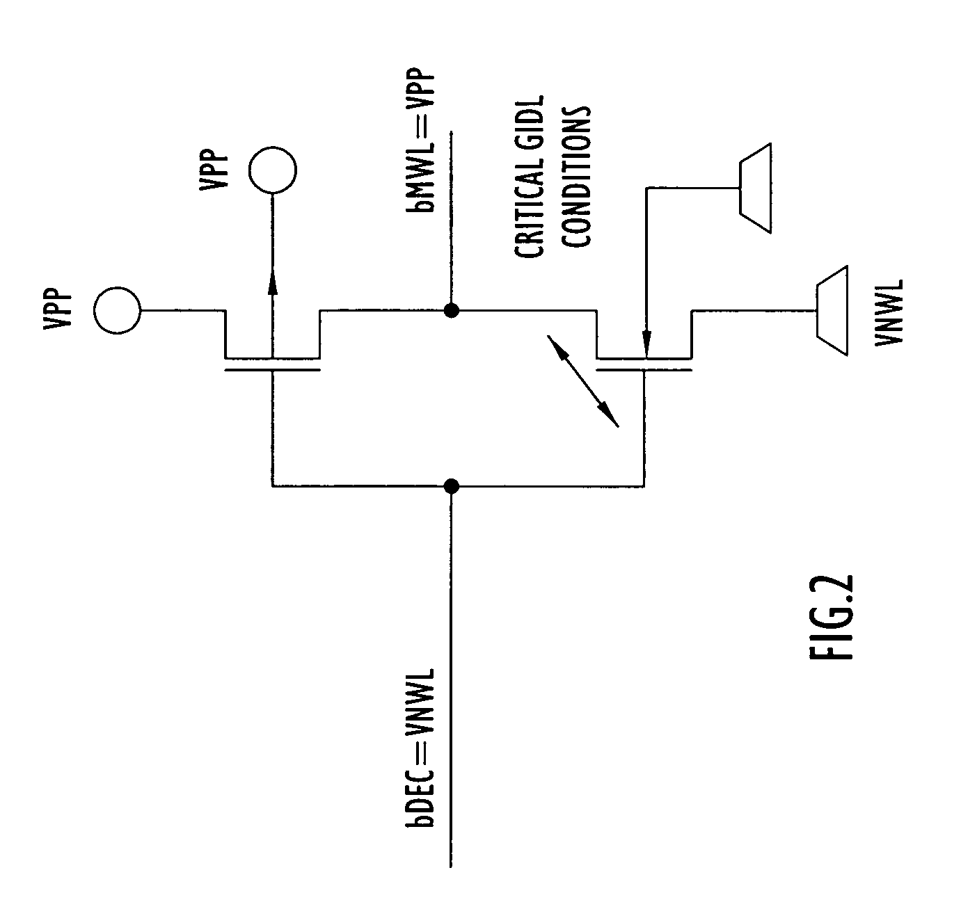
[0013] In a semiconductor memory device, such as a DRAM device, high gate to drain voltages are primarily found in the row path system where boosted voltages and negative voltages are used in the same circuitry. FIGS. 1 and 2 show examples of circuits commonly used in semiconductor memory devices, which circuits present GIDL current issues. FIG. 1 illustrates a master wordline (WL) driver circuit 10 and FIG. 2 illustrates a local WL driver circuit 20. These circuits are used to access rows of memory cells in a memory cell array block. Both of these circuits are instantiated, depending on the memory chip size, more than 10,000 times, for example, in a semiconductor integrated circuit memory device. The WL driver circuit is inactive when the line bMWL is coupled to a voltage VPP, which is greater than VDD for the circuit. Thus, VPP is the boosted WL voltage level (>VDD) and VNWL is the WL low level (usually less than 0 V). In these circuit arrangements, the maximum voltage difference ...


PUM


Abstract

A semiconductor integrated circuit device and method for reducing gate induced leakage current associated with circuits of the semiconductor electrical device, such as a semiconductor integrated circuit memory device. During a standby mode, a voltage supplied to a plurality of circuits is reduced so as to reduce gate induced leakage (GIDL) current associated with said plurality of circuits. During time intervals while in the standby mode, the voltage supplied to a subset of said plurality of circuits is increased to a level necessary for a refresh function associated with said subset of said plurality of circuits and then it is reduced upon completion of said refresh function. In the example a semiconductor memory device, the circuits that are manipulated in this manner are wordline driver circuits. A cyclical self-refresh operation is provided to refresh the WLs associated with subsets of the wordline driver circuits to reduce the overall GIDL current associated with the plurality of wordline driver circuits.

Description

BACKGROUND OF THE INVENTION [0001] The present invention is directed to semiconductor devices, and more particularly to reducing current consumption of a semiconductor memory device. [0002] Semiconductor memory devices, such as dynamic random access memory (DRAM) devices, are manufactured using semiconductor fabrication technologies that are designed to reduce the size of the overall fabricated device. With the advancement of semiconductor fabrication technologies to smaller feature sizes, the ratio of so-called “leakage current” to overall operating current increases significantly. Leakage current is produced by circuits in the semiconductor device when certain voltage conditions associated with the circuit are present. There is also a trend in which semiconductor devices are to be designed to have minimal standby power consumption for use in mobile battery-powered host devices in order to support longer battery-powered operations. Thus, a tension exists between designing the small...

Claims


Application Information

Patent Timeline
IPC IPC(8): G11C5/14G11C7/00
CPCG11C5/147G11C8/08G11C11/406G11C11/40615G11C11/4085G11C29/783G11C2211/4067G11C2211/4068
Inventor SCHNEIDER, HELMUTSTREIF, HARALD
Owner POLARIS INNOVATIONS
Why Eureka
Eureka Blog
Learn More