

Enhanced thin film deposition
a technology of enhanced thin film and deposition temperature, applied in chemical vapor deposition coating, electrical equipment, coatings, etc., can solve the problems of limiting the maximum deposition temperature, limiting the growth temperature, and still affecting the impurity content of ald films
- Summary
- Abstract
- Description
- Claims
- Application Information
AI Technical Summary
Problems solved by technology
Method used
Image

Examples
Embodiment Construction
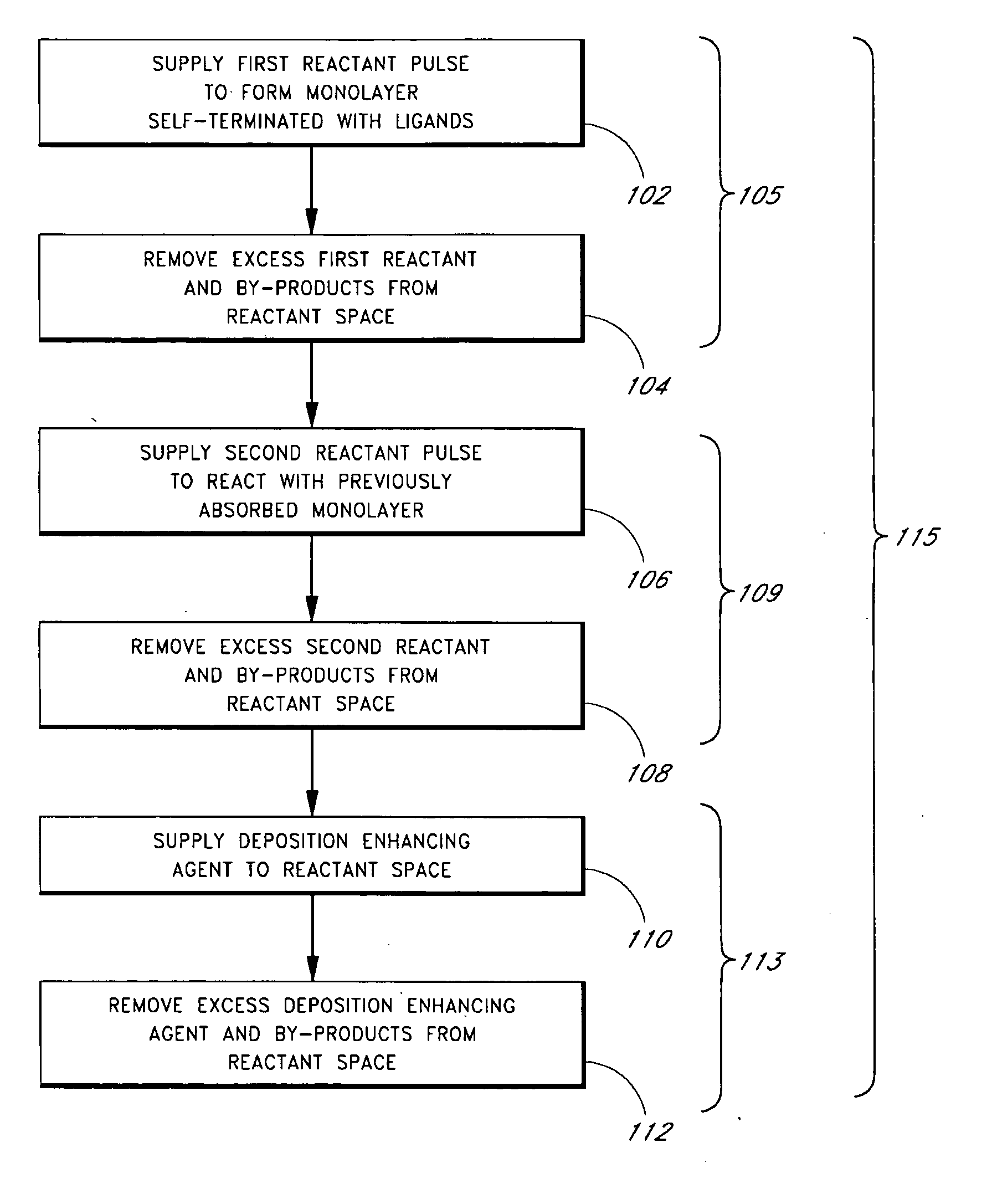
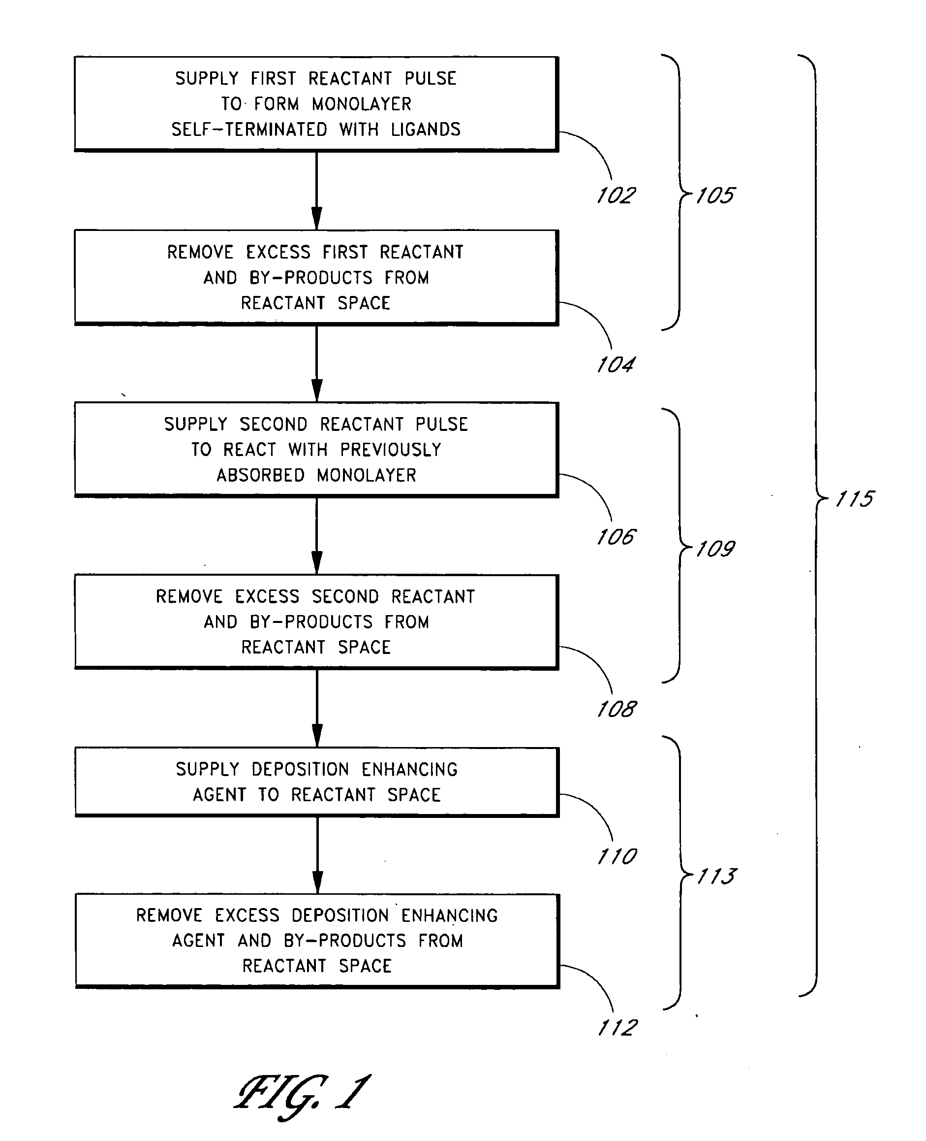
[0023] The present invention advantageously enables thin film formation at lower temperatures with reduced impurity levels by employing a deposition enhancing agent. In some preferred embodiments, the deposition enhancing agents are hydrocarbons, more preferably unsaturated hydrocarbons such as alkanes, alkenes and alkynes.
Definitions
[0024] In context of the present invention, “an ALD process” generally refers to a process for producing thin films over a substrate in which a thin film is formed molecular layer by molecular layer due to self-saturating chemical reactions. The general principles of ALD are disclosed, e.g., in U.S. Pat. Nos. 4,058,430 and 5,711,811, the disclosures of which are incorporated herein by reference. In an ALD process, gaseous reactants, i.e., precursors, are conducted into a reaction chamber of an ALD type reactor where they contact a substrate located in the chamber to provide a surface reaction. The pressure and the temperature of the reaction chamber ...
PUM
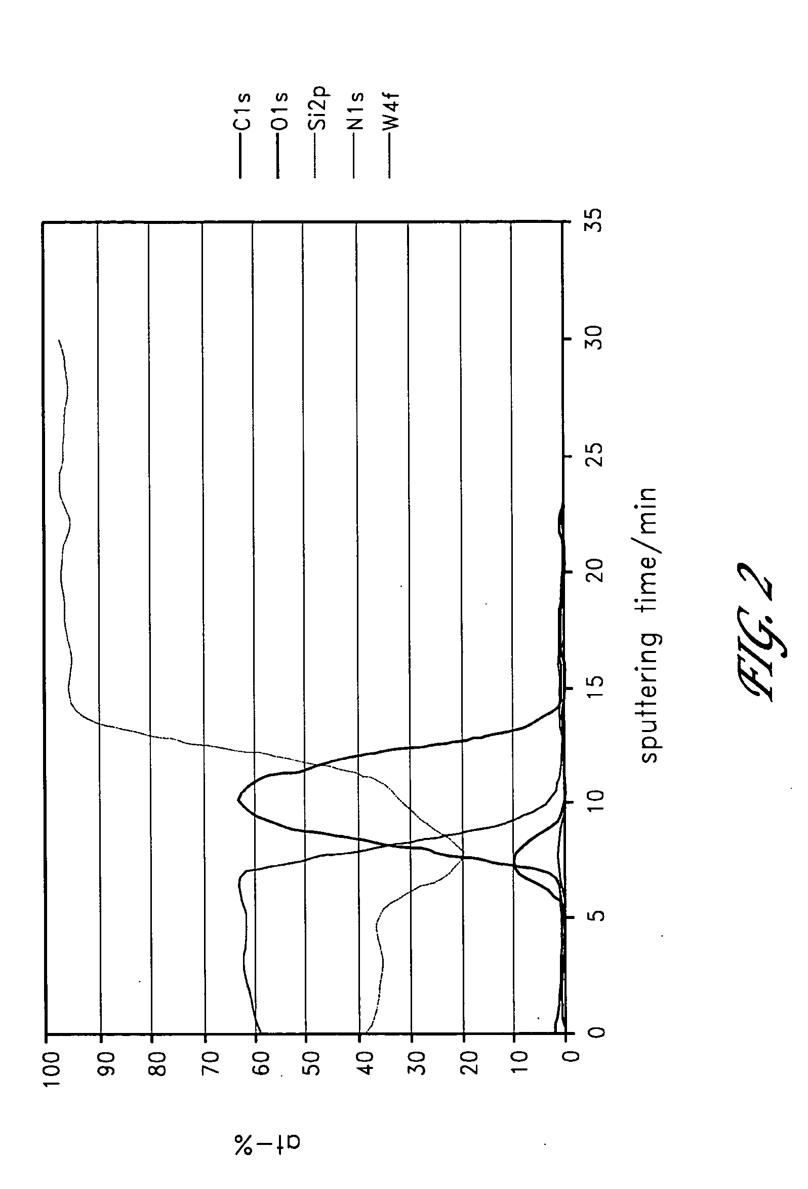
| Property | Measurement | Unit |
|---|---|---|
| decomposition temperature | aaaaa | aaaaa |
| thickness | aaaaa | aaaaa |
| thickness | aaaaa | aaaaa |
Abstract
Description
Claims
Application Information