

Method for treatment of samples for auger electronic spectrometer (AES) in the manufacture of integrated circuits
- Summary
- Abstract
- Description
- Claims
- Application Information
AI Technical Summary
Benefits of technology
Problems solved by technology
Method used
Image

Examples
Embodiment Construction
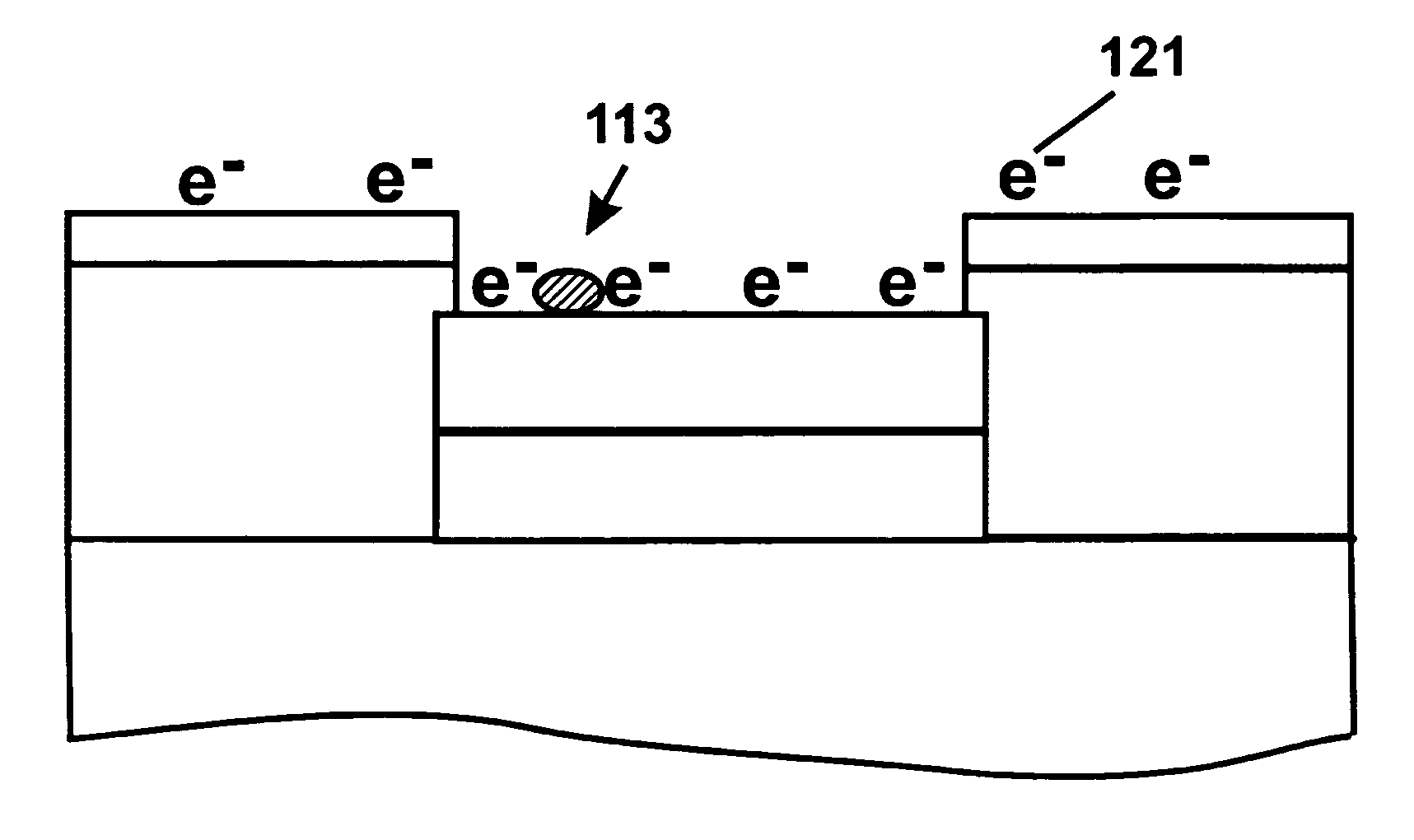
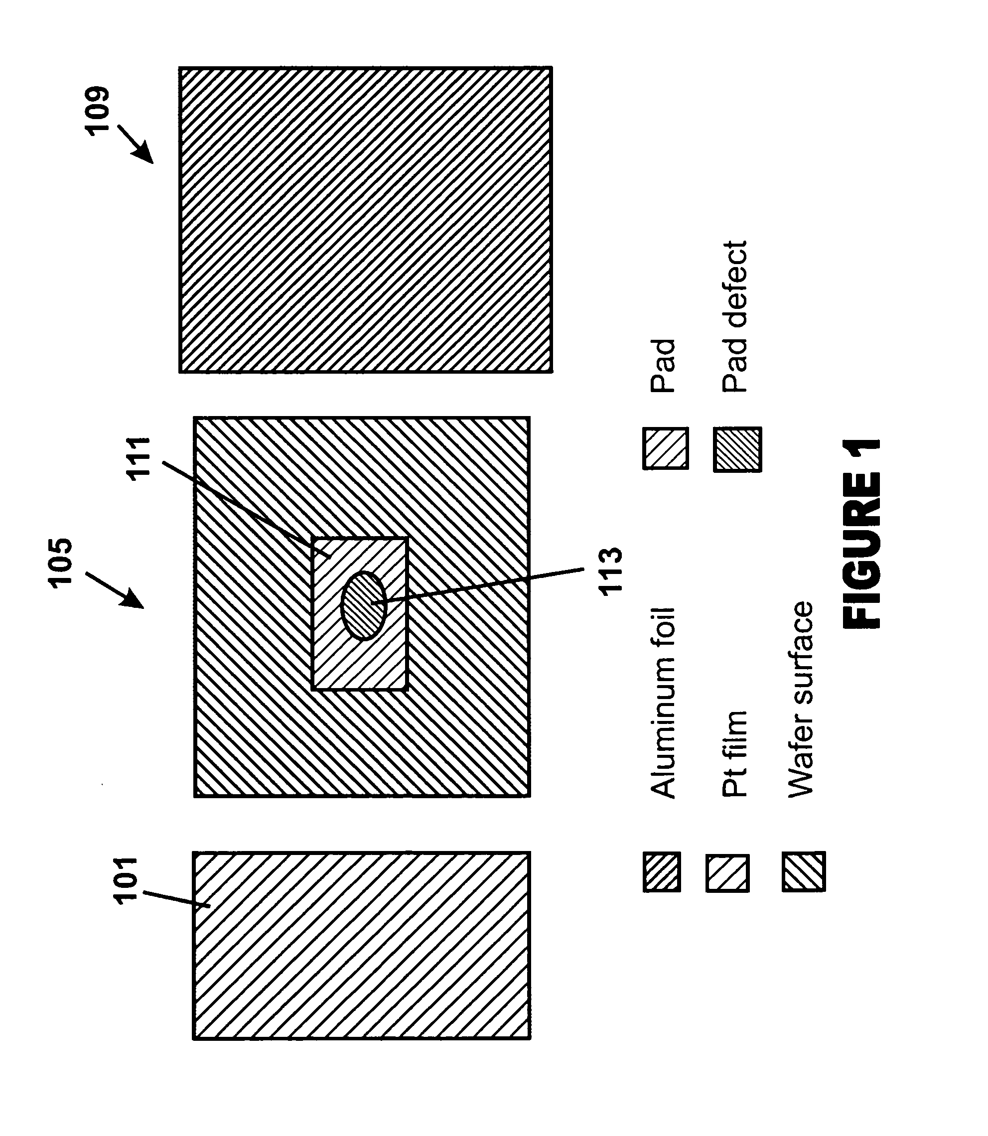
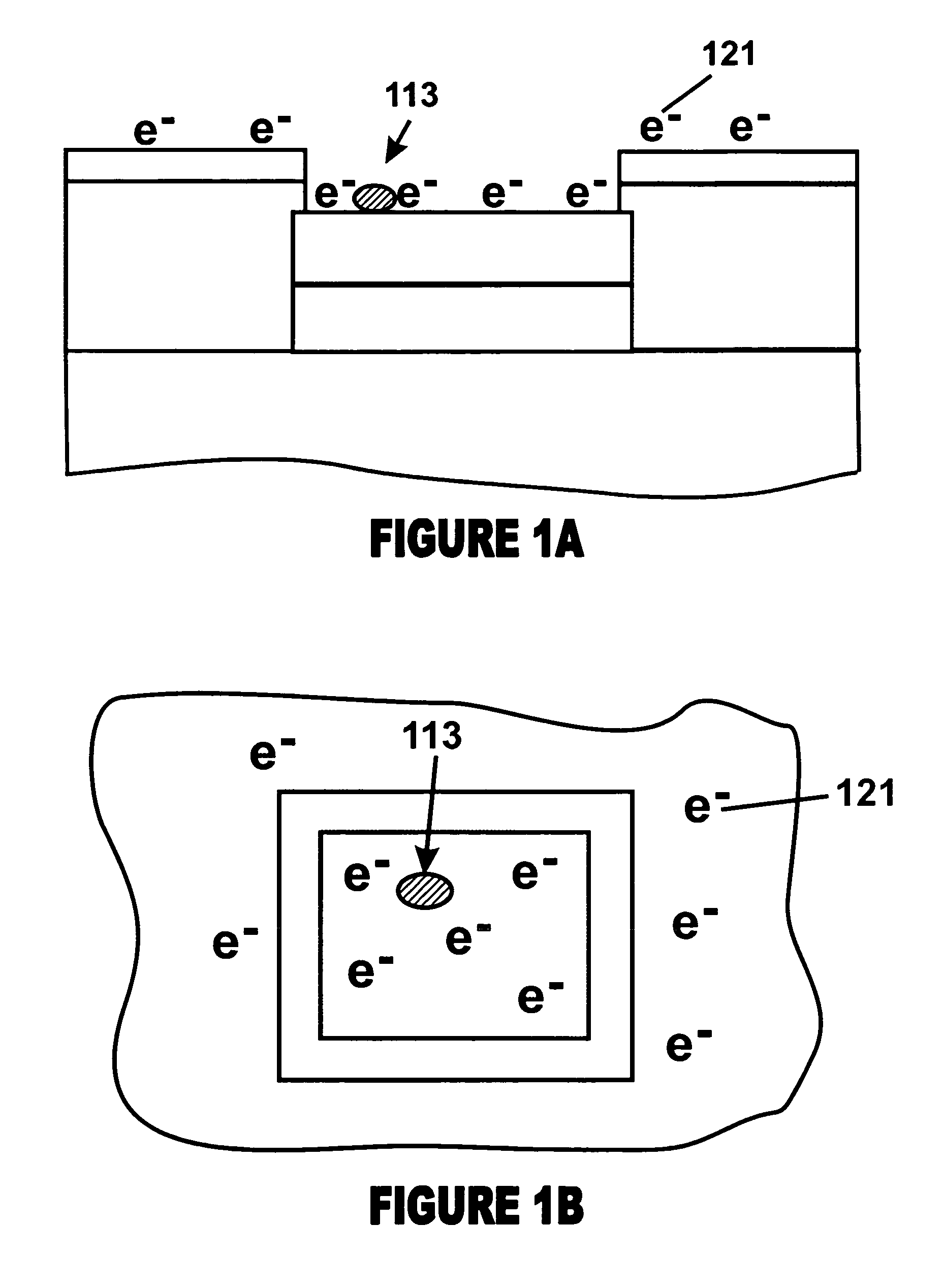
[0020] According to the present invention, techniques for processing integrated circuits for the manufacture of semiconductor devices are provided. More particularly, the invention provides a method and apparatus for preparing samples for an Auger Electronic Spectrometer for the manufacture of integrated circuit devices, but it would be recognized that the invention has a much broader range of applicability. As merely an example, these sample preparation techniques can lead to identifying particulate contamination and / or residues, which lead to lower device yields and other reliability problems.
[0021] As background information, we have discovered that pad surface quality is a frequently monitored item in a semiconductor foundry. That is, pad surface quality is often monitored for contamination or residues on pad surface, which often bring about a series of bonding issues such as bondability and poor electrical contact. Among the many surface analysis tools, AES (Auger Electronic Sp...
PUM
 Abstract
Description
Claims
Application Information