

Semiconductor surface protecting sheet and method
a technology of surface protection sheet and membrane, which is applied in the direction of heat-activated film/foil adhesive, film/foil adhesive, manufacturing tools, etc., can solve the problems of reducing the ability of the current pressure-sensitive adhesive surface protection sheet, and reducing the transverse strength of the wafer. , to achieve the effect of adequate conformability and sufficient rigidity
Inactive Publication Date: 2007-06-28
3M INNOVATIVE PROPERTIES CO
View PDF60 Cites 17 Cited by
- Summary
- Abstract
- Description
- Claims
- Application Information
AI Technical Summary
Benefits of technology
[0006] It is an object of one aspect of the present invention to provide a semiconductor surface protecting method employing a material having an adequate conformability for irregularities on a semiconductor wafer circuit side and sufficient rigidity as a support during grinding, and which does not become fluid with repeated temperature increase, as well as a surface protecting sheet which can be used in the method.
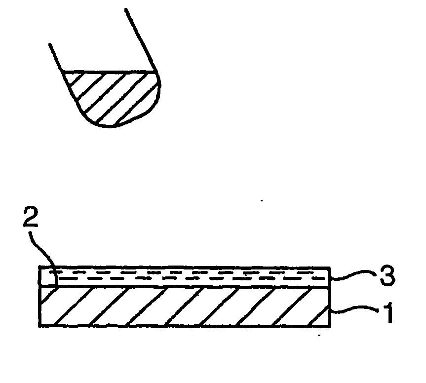
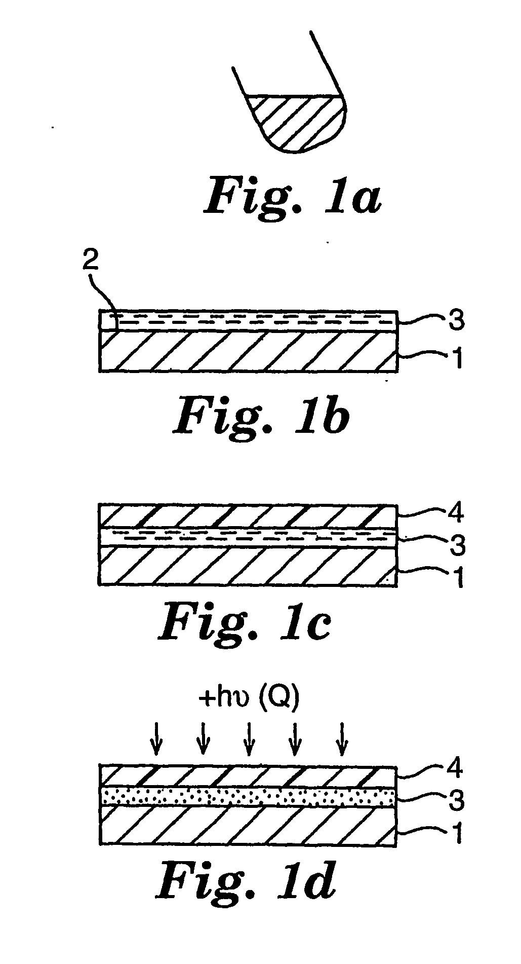
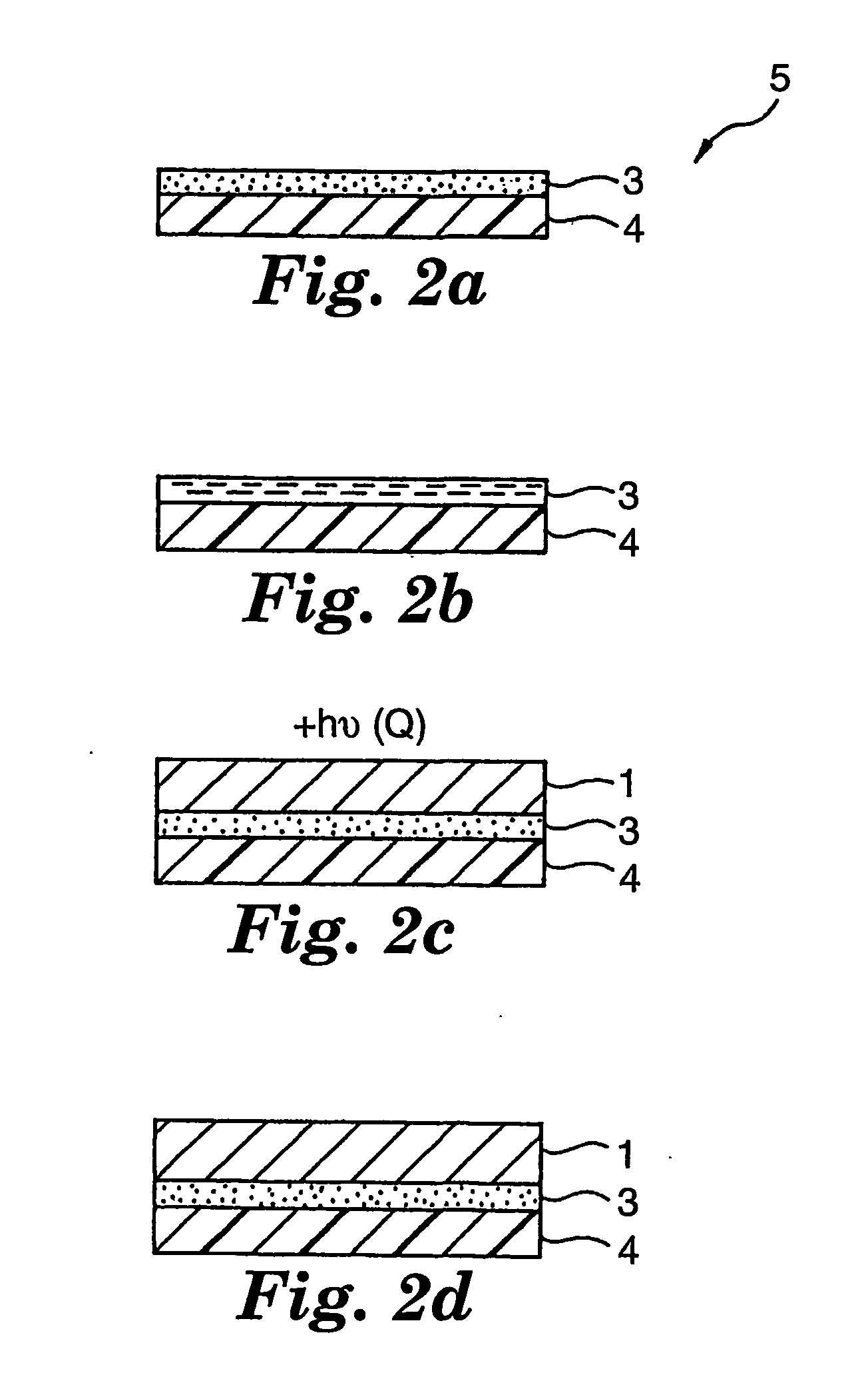
[0020] First, a fluid surface protecting layer material which can be hardened by light or heat is provided (Step (a)). The material of the surface protecting layer may be a liquid at room temperature (about 20-25° C.) or a solid at room temperature which is fluidized by heating. The surface protecting layer 3 material is then evenly coated on the circuit side 2 of a wafer 1 (Step (b)). A polymeric film material 4 is then placed over the protecting layer 3 (Step (c)), and the protecting layer 3 is hardened by ultraviolet rays or heating (Step (d)). During this procedure, care must be taken to avoid inclusion of air at the interface between the protecting layer 3 and the wafer 1, the interface between the protecting layer 3 and the polymeric film material 4, or in the protecting layer 3. Inclusion of air will prevent a smooth grinding surface on the wafer, making it impossible to thinly grind the wafer to an even thickness, or possibly leading to damage of the wafer during grinding. Conducting the procedure in a vacuum can prevent air inclusion.
Problems solved by technology
Presently employed pressure sensitive adhesive surface protecting sheets are limited in their ability to conform to the irregularities of the circuitry on a semiconductor wafer.
As a result, gaps (air pockets) are created between the pressure-sensitive adhesive layer and the circuit side, such that the wafer is not directly supported by the pressure-sensitive adhesive (protective layer) in those areas.
This phenomenon is not a problem if the finished thickness is 150 μM or greater, but if the wafer is thinned to less than 100 μm (especially when finishing to a thickness of 50 μm or less), or if tall protrusions such as bumps are present on the wafer circuit side (for example, at 100 μm or greater), not only is the transverse strength of the wafer reduced considerably, but in severe cases the wafer can even be damaged during grinding.
Also, when a wafer is thinly ground to about 50 μm edge chipping of the wafer or penetration of grinding water between the wafer and surface protecting layer can constitute a problem, but this has also been caused by a lack of adhesion of the surface protecting sheet to the wafer edges.
In addition, with semiconductor wafers which are thin and also have bumps or other protrusions of 100 μm or greater on the circuit side, it is difficult to accomplish grinding by attachment of typical surface protecting sheets.
If this tendency is too strong, however, the wafer can undergo considerable stress and suffer damage when the sheet is removed by peeling from the wafer.
However, an often occurring problem is that the pressure-sensitive adhesive layer is too flexible in the unhardened state during grinding, and the wafer thus suffers damage during grinding.
However, since the pressure-sensitive adhesive is not fluid, its conformability against irregularities on the wafer circuit side is not adequate.
However, the sheet repeatedly melts when the temperature rises above the melting point.
As a result, the temperature increase produced in such steps has caused problems including remelting of the protective sheet.
Method used
View moreImage
Smart ImageViewing Examples

Examples
example 1 (
Ultraviolet Curing Solid Protecting Layer)
[0043]
TABLE 1WeightChemical NameProduct NamePercentUrethane acrylateUV3520TL76.1%Tris(acryloxyethyl)isocyanurateM31519.1%2-Benzyl-2-dimethylamino-1-(4-Irgacure 3694.8%morpholinophenyl)-butanone-1100.0%
example 2 (
Ultraviolet Curing Solid Protecting Layer)
[0044]
TABLE 2WeightChemical NameProduct NamePercentUrethane acrylateUV3510TL76.2%Bisphenol A diacrylateVR9019.0%2-Benzyl-2-dimethylamino-1-(4-Irgacure 3694.8%morpholinophenyl)-butanone-1100.0%
example 3 (
Ultraviolet Curing Solid Protecting Layer)
[0045]
TABLE 3WeightChemical NameProduct NamePercentUrethane acrylateUV3510TL57.1%Bisphenol A diacrylateVR9038.1%2-Benzyl-2-dimethylamino-1-(4-Irgacure 3694.8%morpholinophenyl)-butanone-1100.0%
Login to View More PUM
| Property | Measurement | Unit |
|---|---|---|
| temperature | aaaaa | aaaaa |
| frequency | aaaaa | aaaaa |
| elastic tensile storage modulus | aaaaa | aaaaa |
Abstract
Provided are a semiconductor surface protecting method and surface protecting sheet employing a material having adequate conformability for irregularities on semiconductor wafer circuit sides and sufficient rigidity as a support during grinding, and which does not become fluid with repeated temperature increases. Also provided is a surface protecting sheet for protection of the circuit side in the step of back side grinding of a semiconductor wafer, the surface protecting sheet having a polymeric film material with a surface protecting layer thereon that may become fluid upon heating and which hardens upon exposure to radiation or upon heating.
Description
TECHNICAL FIELD [0001] The present invention relates to a semiconductor surface protecting method and surface protecting sheet for protection of the circuit-containing sides of a semiconductor wafer during the process of back side grinding of the wafers. More specifically, the invention relates to a semiconductor surface protecting method and surface protecting sheet which permits ultrathin back side grinding of semiconductor wafers, or which permits back side grinding of semiconductor wafers having high protrusions such as solder bumps on the circuit side. BACKGROUND [0002] Thinning (also referred to herein as “grinding”) of semiconductor wafers has conventionally been accomplished by “back side grinding” methods whereby the circuit side of a wafer is protected with a surface protecting sheet and the back side opposite the circuit side is ground. The thicknesses of silicon wafers are generally 150 μm on an industrial level, but even thinner wafer thicknesses are desired. When wafer...
Claims
Login to View More Application Information
Patent Timeline
 Patent Type & AuthorityApplications(United States)
IPC IPC(8): H01L21/30H01L21/46B24B7/22B24B37/30B24B55/00C09J7/22C09J7/35H01L21/00H01L21/304H01L21/68
CPCB24B7/228B24B55/00H01L21/67132C09J2461/00C09J2463/00C09J7/0242C09J7/35C09J7/22H01L21/304H01L21/48
InventorNODA
Owner3M INNOVATIVE PROPERTIES CO