Free electron laser

Inactive Publication Date: 2007-07-05
INTEL CORP
View PDF7 Cites 82 Cited by
  • Summary
  • Abstract
  • Description
  • Claims
  • Application Information

AI Technical Summary

Problems solved by technology

These programs require complex integrated circuits (IC's) to operate.
These existing sources are capable of producing the desired wavelengths; however, producing the desired wavelengths using the plasma based sources has several disadvantages, including production of debris that can contaminate and damage the optics used in EUV lithography systems.
In addition, these sources em

Method used


Image

  • Free electron laser
  • Free electron laser
  • Free electron laser

Examples


Embodiment Construction

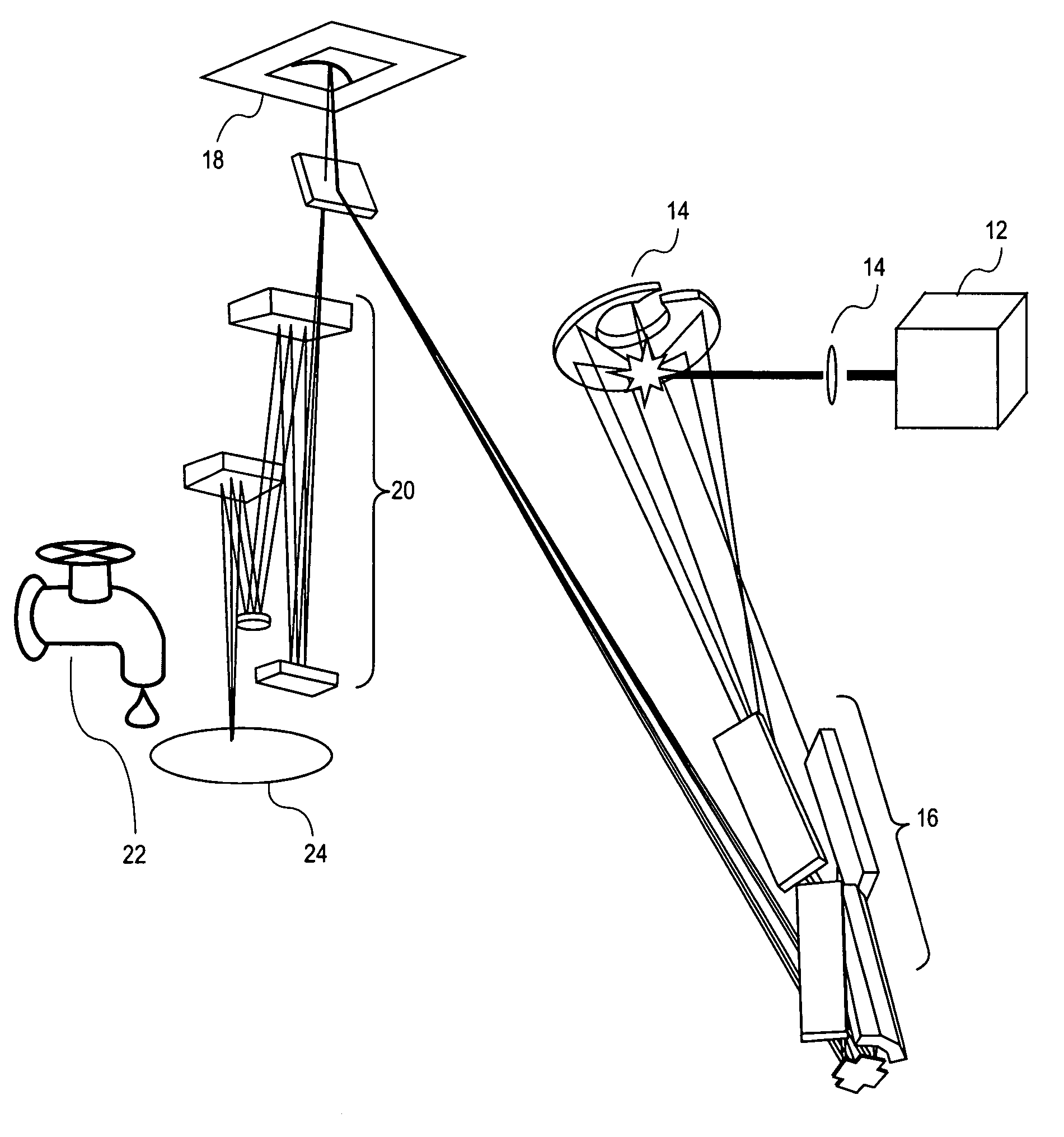
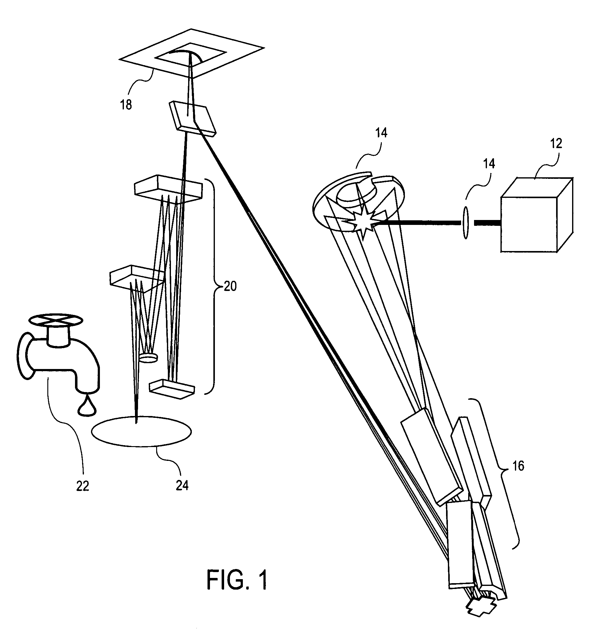
[0019]FIG. 1 illustrates an extreme ultraviolet (EUV) lithography system 10, according to an embodiment of the invention, which can be used in the manufacture of integrated circuits (ICs). The lithography system 10 includes an EUV light source 12, collector optics 14, an illuminator 16, a reflective mask 18, reflective reduction optics 20 and a resist source 22, for the purposes of making lithography patterns on a wafer 24.

[0020] The light source 12 is an EUV radiation light source (i.e., light source 12 radiates light in the 5-20 nm wavelength range). Ideally, the light source 12 produces EUV radiation having an approximately 13.5 nm wavelength. EUV radiation is referred to throughout the specification; however, it will be appreciated by those of skill in the art that EUV radiation also refers to EUV light.

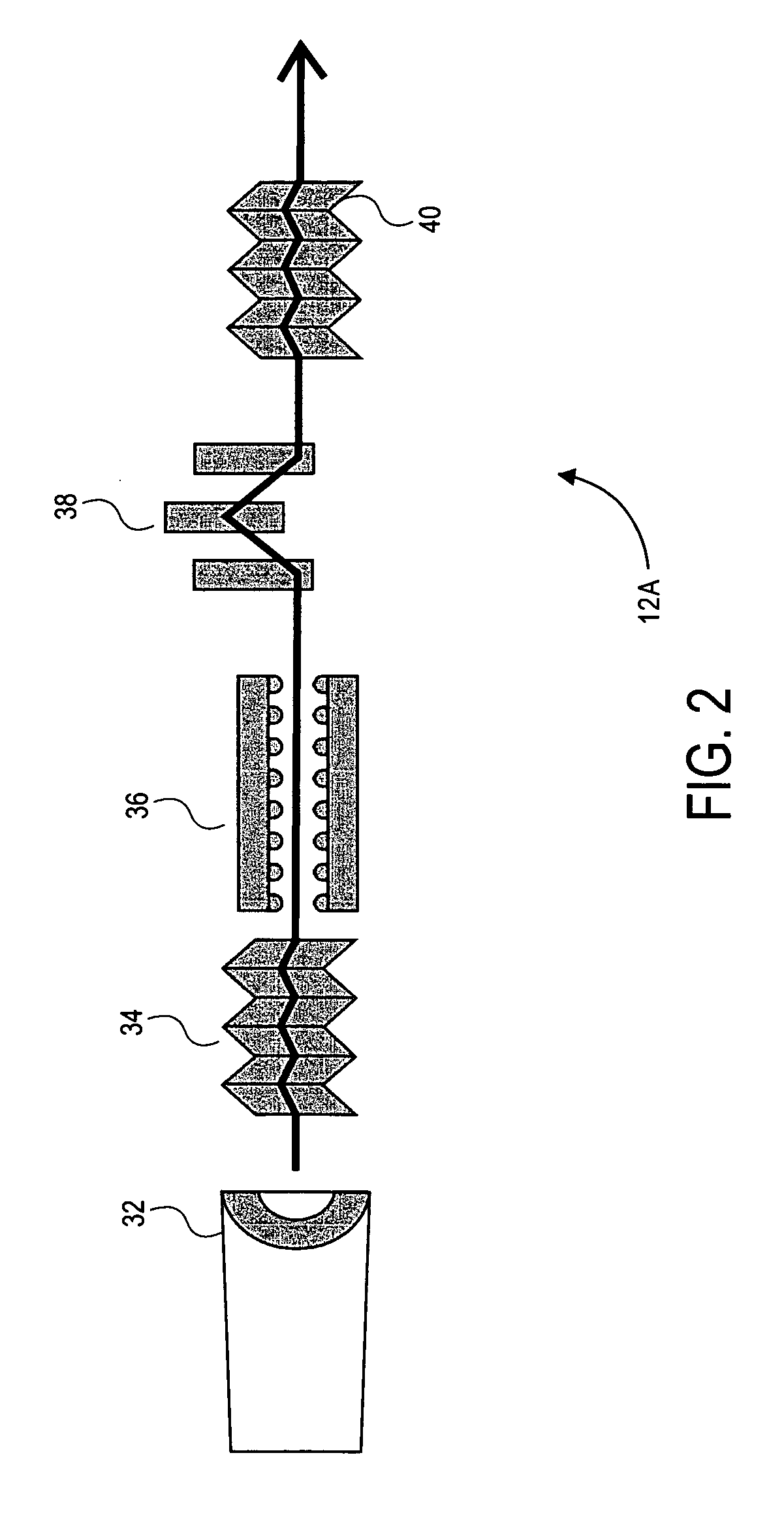
[0021] The collector optics 14 are arranged to collect the EUV radiation from the light source 12 and direct the EUV radiation toward the illuminator 16. The collector optics 1...


PUM


Abstract

A free electron laser is disclosed. The free electron laser separates pulse bunching at a first electron energy from light generation stage at a second electron energy. A first wiggler pulse bunches the electrons and a second wiggler generates light. The first wiggler may be an optical buncher with an injected seed wave, and the second wiggler can be a magnetic wiggler, optical wiggler, resonant transition radiator, parametric radiation radiator, Cerenkov radiation radiator or a Smith-Purcell radiation radiator. The disclosed free electron laser is particularly useful for lithography applications at an extreme ultraviolet wavelength range near 13.5 nm.

Description

FIELD OF THE INVENTION [0001] The present invention relates to the field of free electron lasers and, in particular, to an apparatus and method for attaining extreme ultraviolet (EUV) wavelengths. BACKGROUND OF THE INVENTION [0002] Many every day items, including computers, phones, and even our cars include computer chips. Programs run on computer chips, providing these items with electronic functionality. These programs require complex integrated circuits (IC's) to operate. These circuits are built in layers on a silicon wafer using chemicals, gases and light. A layer of silicon oxynitride is grown on the silicon wafer and a resist is deposited on the wafer. In a photolithography process, UV light is passed through a patterned mask (or stencil) onto the resist-coated wafer. The light reacts with the resist, leaving features of the IC on the wafer. The unexposed areas (resist and silicon dioxide) are removed. This process is repeated several times to form several layers of circuit f...

Claims


Application Information

Patent Timeline
IPC IPC(8): A61N5/00
CPCG03F7/70025H05H7/04H01S3/0903G03F9/7065
Inventor GOLDSTEIN, MICHAELWILLIAMS, DAVID L.
Owner INTEL CORP
Why Eureka
Try Eureka