Tin-bismuth (Sn-Bi) family alloy solder and semiconductor device using the same

a technology of alloy solder and semiconductor, which is applied in the direction of soldering apparatus, metal working apparatus, manufacturing tools, etc., can solve the problems of easy cracks at the junction to which stress is applied, easy deformation of the junction, and brittle junction, etc., to achieve the effect of increasing the reliability of the junction

Inactive Publication Date: 2007-07-05
SAMSUNG ELECTRONICS CO LTD
View PDF14 Cites 59 Cited by
  • Summary
  • Abstract
  • Description
  • Claims
  • Application Information

AI Technical Summary

Benefits of technology

[0003]Example embodiments of the present invention relate to an alloy solder and a semiconductor device using the alloy solder. Other example embodiments relate to an alloy solder capable of increasing reliability of a junction between a semiconductor chip and a substrate.

Problems solved by technology

According to the flip chip mounting technology disclosed in the conventional art, before a solder bump is formed on a semiconductor chip, an under bump metal (UBM) layer may be formed by plating a wafer unit on a bonding pad of the semiconductor chip, which may be costly.
If a relatively large amount of the intermetallic compound layer AuSn4 is formed in the junction, the junction may be deformed easily by external forces, because the junction is brittle mechanically.
If a temperature change test is conducted, cracks may easily occur at the junction to which stresses are applied due to the difference between the thermal expansion ratios of the semiconductor chip and substrate.
The reliability of the junction may thereby decrease.

Method used


Image

  • Tin-bismuth (Sn-Bi) family alloy solder and semiconductor device using the same
  • Tin-bismuth (Sn-Bi) family alloy solder and semiconductor device using the same
  • Tin-bismuth (Sn-Bi) family alloy solder and semiconductor device using the same

Examples


Embodiment Construction

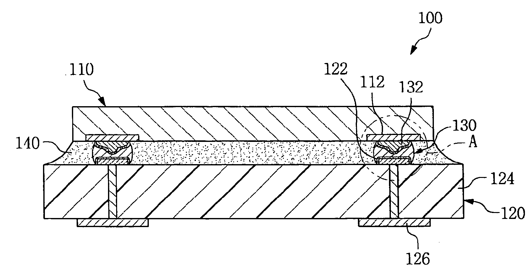
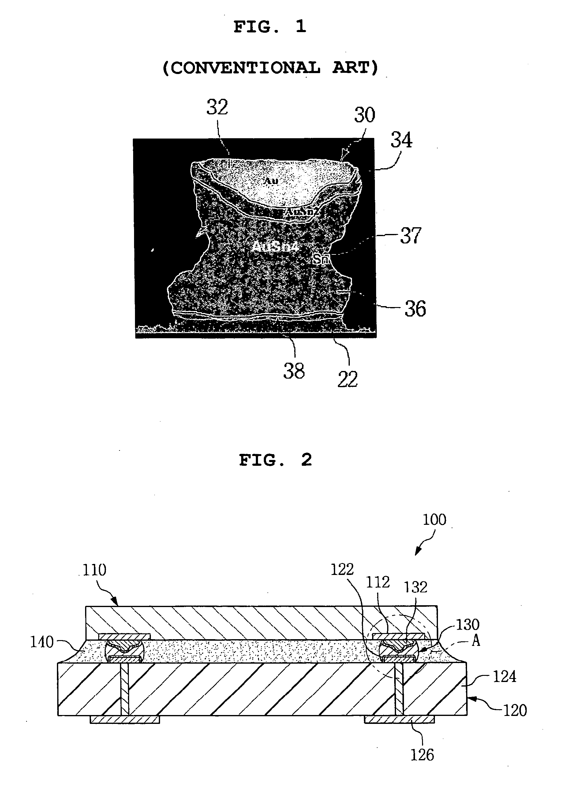
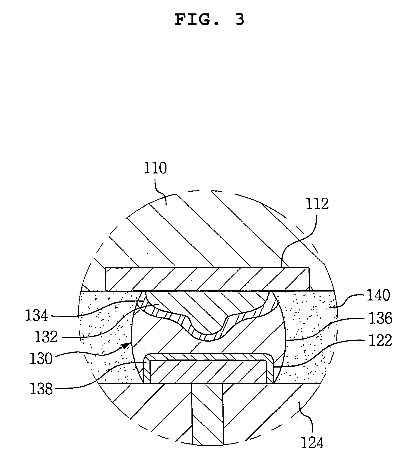
[0022]Various example embodiments of the present invention will now be described more fully with reference to the accompanying drawings, in which some example embodiments of the present invention are shown. Example embodiments of the present invention may, however, be embodied in many different forms and should not be construed as limited to the example embodiments set forth herein. Rather, these example embodiments are provided so that this disclosure will be thorough and complete, and will fully convey the scope of the present invention to those skilled in the art.

[0023]In the description, well-known structures and processes have not been described or illustrated to avoid obscuring example embodiments of the present invention. In the drawings, some elements are exaggerated or only outlined in brief, and thus may not be drawn to scale for simplicity and clarity of illustration. The same reference symbols are given to the same or corresponding elements in the drawings.

[0024]It will ...


PUM

PropertyMeasurementUnit
total volumeaaaaaaaaaa
volumeaaaaaaaaaa
conductiveaaaaaaaaaa

Abstract

Example embodiments of the present invention relate to an alloy solder and a semiconductor device using the alloy solder. Other example embodiments relate to an alloy solder capable of increasing reliability of a junction between a semiconductor chip and a substrate. According to still other example embodiments of the present invention, there may be a tin-bismuth (Sn—Bi) family alloy solder between a semiconductor chip and a substrate, and a semiconductor device using the alloy solder. The semiconductor device may include a semiconductor chip formed with a plurality of gold (Au) bumps, a substrate having metal wirings connected to the gold (Au) bumps, and a junction including a tin-bismuth (Sn—Bi) family alloy solder interposed between and connecting the gold (Au) bump and the metal wiring.
The formation of a relatively large amount of AuSn4 intermetallic compound may be inhibited in the junction because gold (Au) may not easily diffuse into a tin-bismuth (Sn—Bi) family alloy solder of a liquid state during a reflow process for connecting the semiconductor chip and substrate. Therefore, most of the junction may be retained as the tin-bismuth (Sn—Bi) family alloy solder.

Description

PRIORITY STATEMENT[0001]This U.S. non-provisional application claims priority under 35 U.S.C. §119 from Korean Patent Application No. 2005-133620, filed on Dec. 29, 2005, in the Korean Intellectual Property Office (KIPO), the entire contents of which are herein incorporated by reference.BACKGROUND[0002]1. Field[0003]Example embodiments of the present invention relate to an alloy solder and a semiconductor device using the alloy solder. Other example embodiments relate to an alloy solder capable of increasing reliability of a junction between a semiconductor chip and a substrate.[0004]2. Description of the Related Art[0005]In response to a recent trend towards miniaturization of electronic devices, various studies are being conducted in the semiconductor industry to mount more semiconductor chips on a smaller substrate by fabricating smaller and highly integrated semiconductor packages. Flip chip mounting technology has been used for mounting such semiconductor devices. Flip chip mou...

Claims


Application Information

Patent Timeline
Patent Type & Authority Applications(United States)
IPC IPC(8): H01L23/48
CPCB23K35/025B23K35/262H01L24/13H01L24/11H01L2224/32225H01L2924/014H01L2924/01047H01L2924/01033H01L2924/01006H01L2924/00013H05K3/3463H01L2924/01327H01L2924/01322H01L2924/01082B23K35/264B23K2201/40C22C12/00C22C13/00C22C13/02C22C30/02C22C30/04C22C30/06H01L2224/1134H01L2224/13144H01L2224/16225H01L2224/73204H01L2924/01013H01L2924/01029H01L2924/0103H01L2924/01078H01L2924/01079H01L2224/13099H01L2924/00B23K2101/40H01L24/05H01L2224/05571H01L2224/05573H01L2224/05624H01L2224/11H01L2224/13H01L2924/15787H01L2924/00014H01L23/48
Inventor KANG, UU-BYUNGKWON, YONG-HWANLEE, JONG-HOLEE, CHUNG-SUN
Owner SAMSUNG ELECTRONICS CO LTD
Why Eureka
Try Eureka