High dielectric antenna substrate and antenna thereof

Active Publication Date: 2007-07-05
IND TECH RES INST
View PDF8 Cites 3 Cited by
  • Summary
  • Abstract
  • Description
  • Claims
  • Application Information

AI Technical Summary

Benefits of technology

[0017]According to the embodiments of the present invention, by using a high dielectric material, the antenna area can be reduced, the material cost can be saved, and the assembly cost can be decreased.
[0018]According to the embodiments of the present invention, the capacitor is embedded within the substrate. As many optional capacitances can b

Problems solved by technology

However, with the trend of electronic products becoming light, thin, short, and small, the components for electronic products must also consider this trend in design.
However, the installation of the discrete capacitor increases the cost, and the capacitance coupling magnit

Method used


Image

  • High dielectric antenna substrate and antenna thereof
  • High dielectric antenna substrate and antenna thereof
  • High dielectric antenna substrate and antenna thereof

Examples


first embodiment

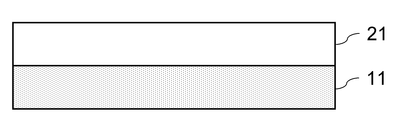
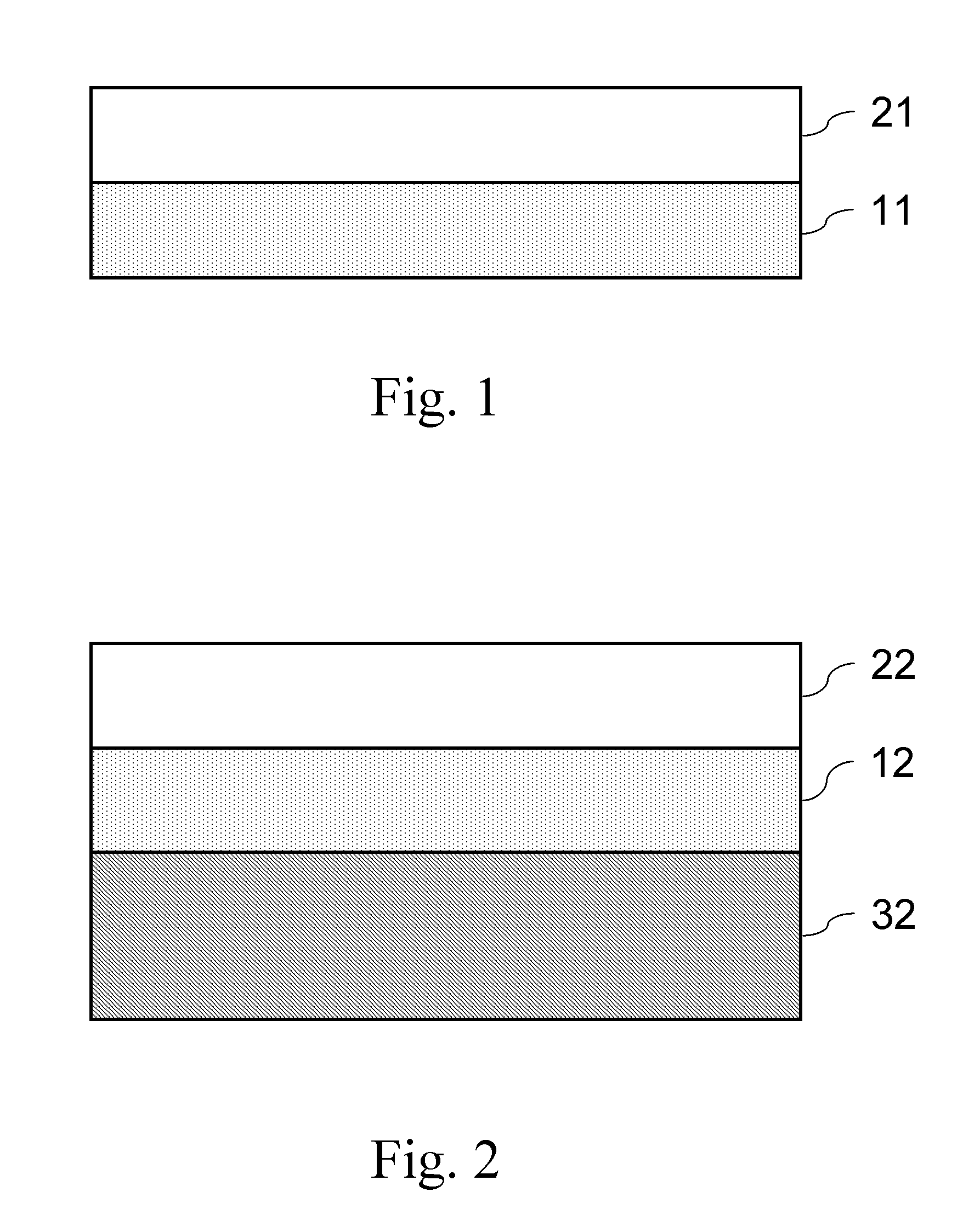
[0045]FIG. 1 is a schematic structural diagram of a high dielectric antenna substrate according to the present invention. As shown in FIG. 1, the antenna substrate is a composite substrate including a first dielectric layer 11 and a second dielectric layer 21. The first dielectric layer 11 is made of a high dielectric material and has a first dielectric constant. The second dielectric layer 21 having a second dielectric constant formed on one surface of the first dielectric layer 11. The second dielectric constant of the second dielectric layer 21 is lower than the first dielectric constant of the first dielectric layer 11.

second embodiment

[0046]Referring to FIG. 2, it is a schematic structural diagram of the high dielectric antenna substrate according to the present invention. As shown in FIG. 2, the antenna substrate is a composite substrate including a first dielectric layer 12 and a second dielectric layer 22. The first dielectric layer 12 is made of a high dielectric material and has a first dielectric constant. The second dielectric layer 22 having a second dielectric constant formed on one surface of the first dielectric layer 12. It further comprises a substrate 32, formed on the other surface of the first dielectric layer 12. The substrate 32 can be, for example, an organic substrate, such as a glass-fiber substrate (FR4 substrate). The first dielectric layer 12 is made of a high dielectric material, and has a first dielectric constant. The second dielectric layer 22 has a second dielectric constant. The second dielectric constant of the second dielectric layer 22 is lower than the first dielectric constant o...

third embodiment

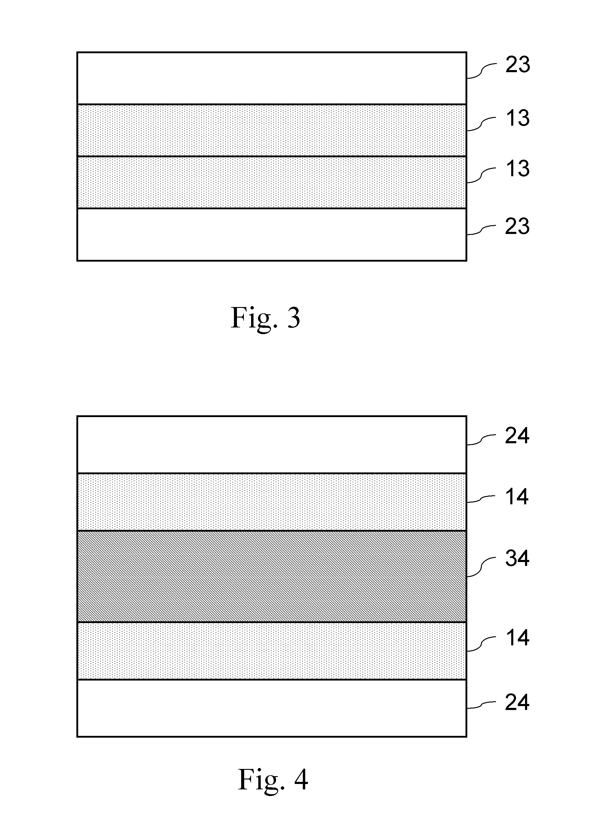
[0047]Referring to FIG. 3, it is a schematic structural diagram of the high dielectric antenna substrate according to the present invention. As shown in FIG. 3, the antenna substrate is a composite substrate including two first dielectric layers 13 and two second dielectric layers 23. The first dielectric layers 13 are made of a high dielectric material, and have a first dielectric constant respectively. One surface of each first dielectric layer 13 contacts and overlays each other. The two second dielectric layers 23, having a second dielectric constant, are formed on the other surfaces of the first dielectric layers 13 respectively. The second dielectric constant is lower than the first dielectric constant.


PUM


Abstract

A high dielectric antenna substrate and antenna thereof are provided. The substrate includes a first dielectric layer having a first dielectric constant, and a second dielectric layer having a second dielectric constant. The second dielectric layer is formed on one surface of the first dielectric layer. The second dielectric constant is lower than the first dielectric constant. Furthermore, a first metal layer and a second metal layer are optionally formed on the same surface or two surfaces of the first dielectric layer to compose a capacitor.

Description

CROSS-REFERENCE TO RELATED APPLICATIONS[0001]This non-provisional application claims priority under 35 U.S.C. §119(a) on Patent Application No(s). 094147751 filed in Taiwan, R.O.C. on Dec. 30, 2005, the entire contents of which are hereby incorporated by reference.BACKGROUND OF THE INVENTION[0002]1. Field of Invention[0003]The present invention relates to an organic substrate antenna, and more particularly, to a high dielectric organic substrate antenna.[0004]2. Related Art[0005]Wireless communication technology is accomplished through electromagnetic wave radiation. The generation of electromagnetic waves is substantially a transformation process between an electric field and a magnetic field, so that energy is transferred in space in the form of a wave. The existence of an antenna provides an environment for the changing of the electric field, and the geometric shape of the antenna determines the oscillation space for the electric field. Generally speaking, materials capable of ge...

Claims


Application Information

Patent Timeline
IPC IPC(8): H01Q1/38
CPCH01Q1/38H01Q9/0485H01Q9/0407
Inventor JOW, UEI-MINGCHEN, CHANG-SHENG
Owner IND TECH RES INST
Why Eureka
Try Eureka