Liquid crystal display device and method for fabricating the same

a technology of liquid crystal display and display device, which is applied in the direction of semiconductor devices, instruments, optics, etc., can solve problems such as signal distortion and signal distortion, and achieve the effect of reducing interference effect and preventing signal distortion

Active Publication Date: 2007-07-05
LG DISPLAY CO LTD
View PDF10 Cites 27 Cited by
  • Summary
  • Abstract
  • Description
  • Claims
  • Application Information

AI Technical Summary

Benefits of technology

[0030]The present invention has been made in an effort to solve the aforementioned problems in the conventional art, and has for its object to provide a method for fabricating a liquid crystal display device, which can prevent signal distortion by reducing the interference effect between an active layer and a common electrode.
[0031]It is another object of the present invention to provide a method for fabricating a liquid crystal display device, which can reduce the number of mask processes.

Problems solved by technology

Such an LCD device is usually manufactured by complicated processes including a photolithography process using a mask.
However, in a case where a diffraction exposure is carried out in order to simultaneously pattern the source / drain electrodes and the active layer, as shown in FIG. 2E, the active pattern may be formed wider than the line width of the source / drain electrodes, and this protruded portion may cause signal distortion.
In particular, when a burst inverter method is used, the photocurrent of the active layer is formed when the burst inverter is performed at a predetermined cycle, and the photocurrent causes an interference effect with the metal (outermost common electrode) of adjacent portions, thus causing the signal distortion.

Method used


Image

  • Liquid crystal display device and method for fabricating the same
  • Liquid crystal display device and method for fabricating the same
  • Liquid crystal display device and method for fabricating the same

Examples


Embodiment Construction

[0042]Hereinafter, a method for fabricating a liquid crystal display device in accordance with embodiments of the present invention will be described with reference to the accompanying drawings.

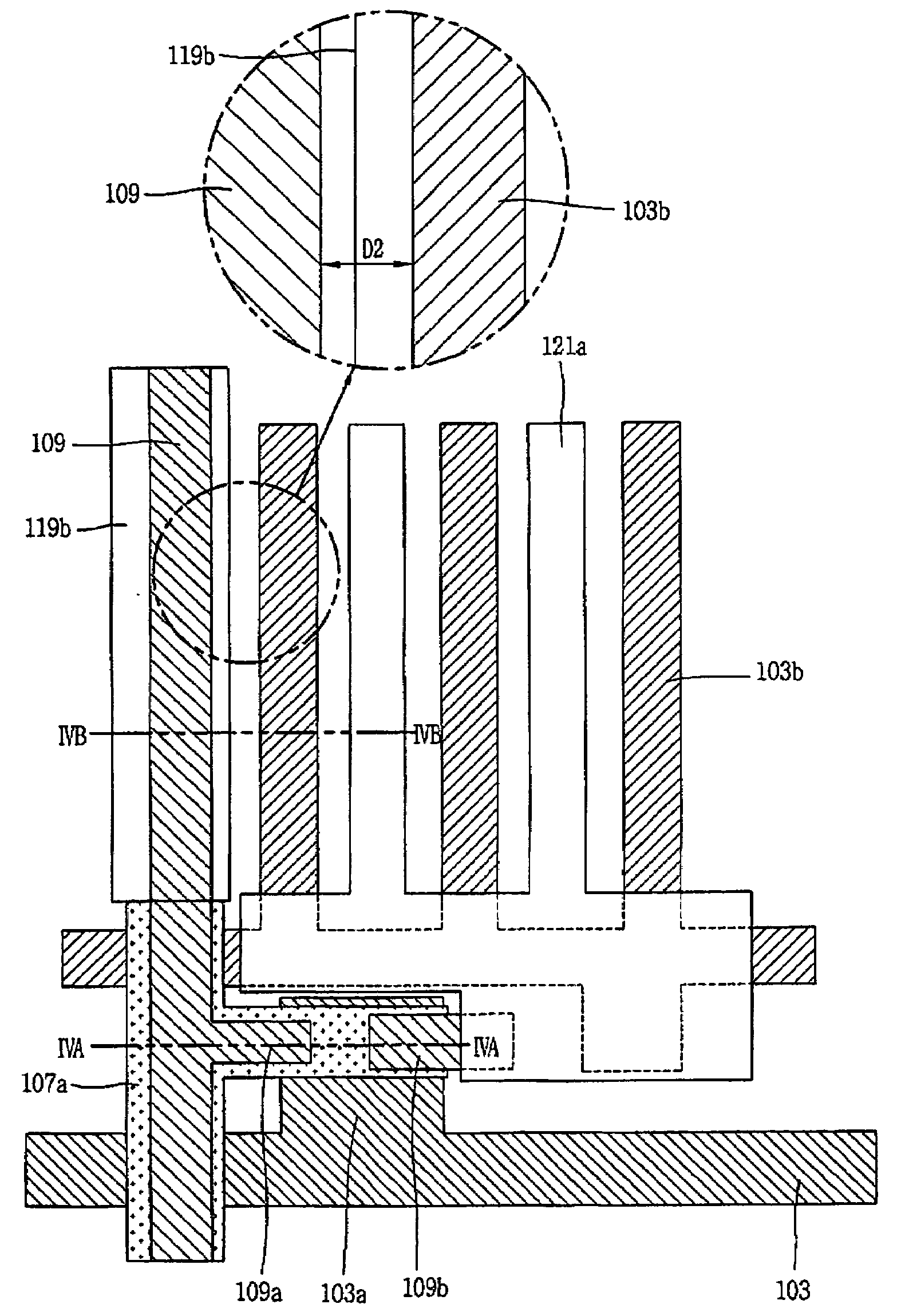
[0043]FIG. 3 is a plane view showing a unit pixel structure of a liquid crystal display device in accordance with an embodiment of the present invention.

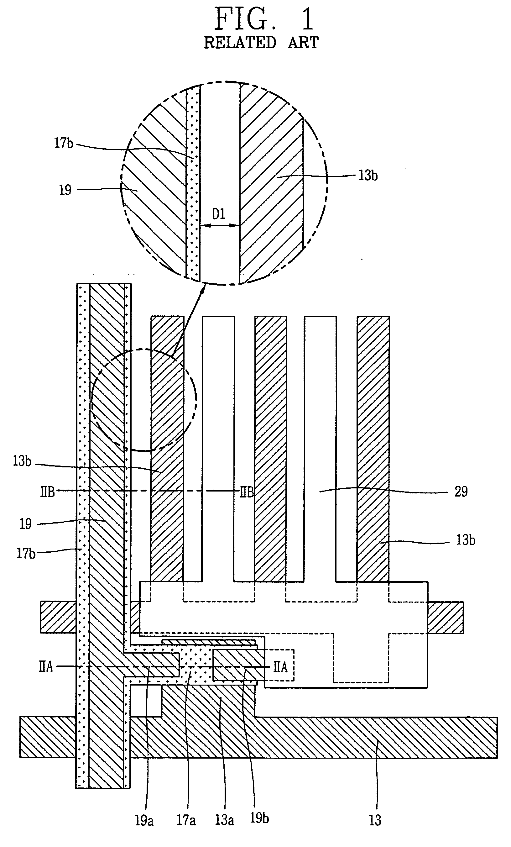
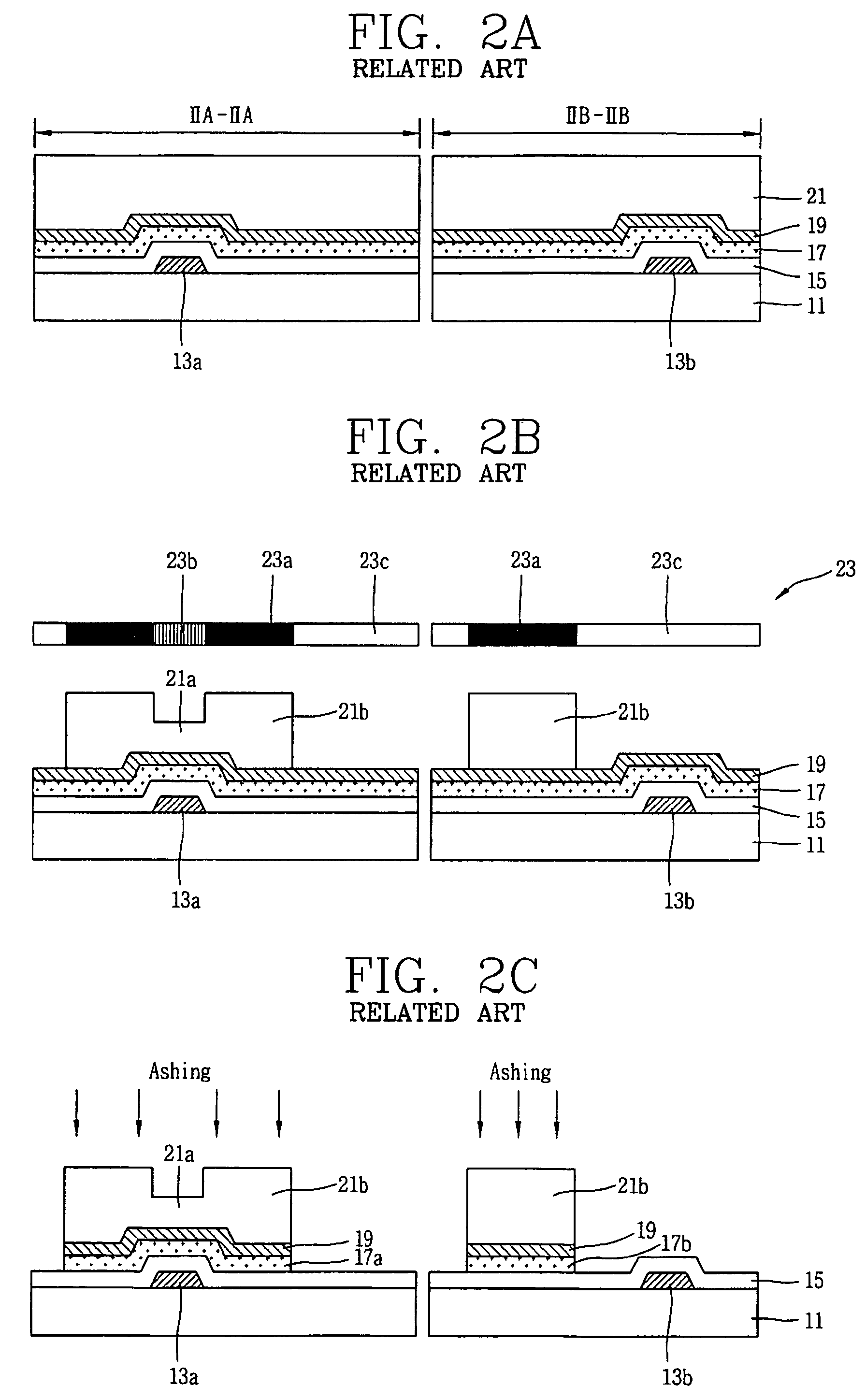
[0044]Referring to FIG. 3, in the liquid crystal display device in the illustrated embodiment, each pixel of the TFT LCD device where N×M pixels are arranged horizontally and vertically includes a TFT (not shown) formed at the crossing of a gate line 13 to which a scan signal is applied from an external driving circuit and a data line 19 to which an image signal is applied.

[0045]The TFT (not shown) includes a gate electrode 103a connected to the gate line 103, an active layer 107 formed on the gate electrode 103 and activated as a scan signal is applied to the gate electrode 103a, and source / drain electrodes 109a and 109b formed on the active...


PUM

PropertyMeasurementUnit
horizontal distanceaaaaaaaaaa
widthaaaaaaaaaa
conductiveaaaaaaaaaa

Abstract

A liquid crystal display device and a method for fabricating the same are provided. The method includes forming a gate line and a data line on a first substrate crossing each other to define a pixel region; forming a gate electrode, a source electrode and a drain electrode of a transistor on the first substrate; forming an active layer below the data line and between the gate electrode and each of the source electrode and the drain electrode, wherein the active layer below the data line has an exposed portion exposed by the data line; removing the exposed portion of the active layer below the data line; and forming a pixel electrode connected to the drain electrode.

Description

[0001]This Nonprovisional Application claims priority under 35 U.S.C. §119(a) on Patent Application No. 10-2005-0136195 filed in Korea on Dec. 30, 2005, the entire contents of which are hereby incorporated by reference.BACKGROUND OF THE INVENTION[0002]1. Field of the Invention[0003]The present invention relates to a liquid crystal display device and a method for fabricating the same. More particularly, the present invention relates to a liquid crystal display device, which can prevent signal distortion by reducing the interference effect between an active layer and a common electrode, as well as a method for fabricating the same.[0004]2. Description of the Related Art[0005]A display device, especially a flat panel display, such as a liquid crystal display (LCD) device, is driven by an active device, such as a thin film transistor (TFT), at each pixel.[0006]This kind of driving method for a display device is usually called an active matrix driving method. In such an active matrix met...

Claims


Application Information

Patent Timeline
Patent Type & Authority Applications(United States)
IPC IPC(8): G02F1/136
CPCG02F1/136227G02F1/136
Inventor YANG, JOON-YOUNG
Owner LG DISPLAY CO LTD
Why Eureka
Try Eureka