Circuit board device with fine conductive structure

Inactive Publication Date: 2007-07-12
PHOENIX PRECISION TECH CORP
View PDF6 Cites 5 Cited by
  • Summary
  • Abstract
  • Description
  • Claims
  • Application Information

AI Technical Summary

Benefits of technology

[0007]Accordingly, it is an objective of the present invention to provide a circuit board device with a fine conductive structure, through which stress strength of the fine conductive structure can be reinforced such that miniature circuit break in the fine conductive structure can be prevented.
[0008]It is another objective of the present invention to provide a circuit board device with a fine conductive structure, through which electrical connection quality between layers of the circuit board can be improved.
[0009]A further objective of the present invention is to provide a circuit board device with a fine conductive structure, through which stress strength of stacked conductive structure can be reinforced and electrical connection quality between layers of a circuit board can be improved.
[0015]According to the present invention, since the fine conductive structure is made of conductive material with high ductility, stress strength of the fine conductive structure can be reinforced. As a result, the miniature circuit break in the prior art is prevented from occurring and the electrically connecting quality in the circuit board is improved.

Problems solved by technology

However, with lead free requirement of the industry and demand for much smaller size of conductive vias, miniature circuit break often occurs inside conductive vias made of copper due to limited ductility and tensile strength of copper.
Particularly, stacked vias of a multi-layer circuit board are much easier to crack if they are subjected to heat stress, which thus adversely affects the electrical connection between different circuit layers and reduces the product reliability.

Method used


Image

  • Circuit board device with fine conductive structure
  • Circuit board device with fine conductive structure
  • Circuit board device with fine conductive structure

Examples


first embodiment

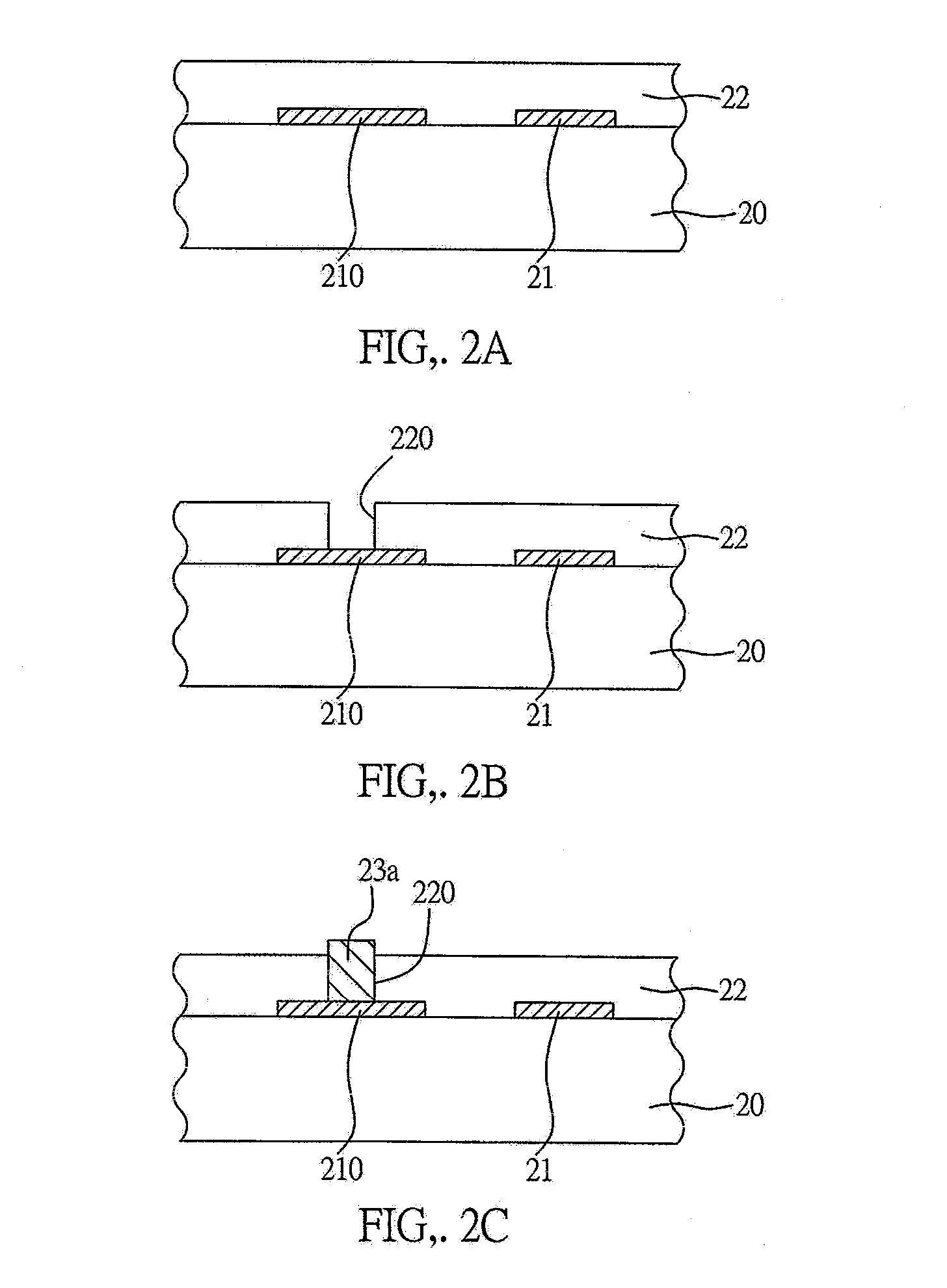
[0023]FIGS. 2A to 2D are sectional diagrams showing a fabrication method of a circuit board device with a fine conductive structure. In the present embodiment, the fine conductive structure has a conductive via structure.

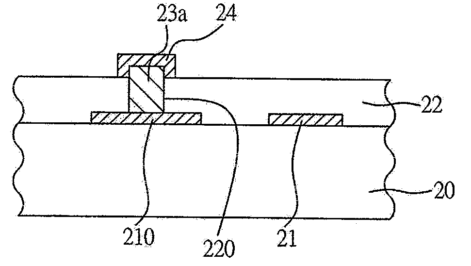
[0024]Referring to FIG. 2A, a circuit board 20 having at least a circuit layer 21 is provided and a first dielectric layer 22 is formed on surfaces of the circuit board 20 and the circuit layer 21. The circuit layer 21 comprises at least one electrically conductive pad 210. The circuit layer 21 can be made of copper. The first dielectric layer 22 can be made of photosensitive or non-photosensitive organic resin or epoxy resin comprising glass fiber, such as ABF (Ajinomoto Build-up Film), BCB (Benzocyclo-buthene), LCP(Liquid Crystal Polymer), PI(Polyimide), PPE(Polyphenylene Ether), PTFE(Polytetrafluoroethylene), FR4, FR5, BT (Bismaleimide Triazine) and Aramide.

[0025]Referring to FIG. 2B, an opening 220 is formed in the first dielectric layer 22 corresponding in posi...

second embodiment

[0031]FIGS. 3A and 3B are sectional diagrams of a circuit board device with a fine conductive structure according to a second embodiment of the present invention. The difference of the circuit board device of the present embodiment from that of the first embodiment is the electrically conductive pad has a recess portion formed on surface thereof so as to increase bonding area between the electrically conductive pad and the fine conductive structure.

[0032]Referring to FIG. 3A, the first dielectric layer 22 is formed on surface of the circuit board 20 having the circuit layer 21 and the opening 220 is formed in the first dielectric layer 22 corresponding in position to the electrically conductive pad 210 of the circuit layer 21. The electrically conductive pad 210 has a recess portion 210a formed on the surface thereof. The recess portion 210a can have such as an arc-shaped recess 210a not penetrating the electrically conductive pad 210.

[0033]Referring to FIG. 3B, the first fine condu...

third embodiment

[0034]FIG. 4 shows a circuit board device according to a third embodiment of the present invention. In the present embodiment, the fine conductive structure is formed inside a multi-layer circuit board.

[0035]As shown in FIG. 4, a second dielectric layer 22′ is further formed on surfaces of the conductive pad 24 and the dielectric layer 22. The second dielectric layer 22′ has an opening 220′ formed therein to expose the conductive pad 24. A second fine conductive structure 23a′ is formed in the opening 220′ and electrically connected to the conductive pad 24. The top surface of the second fine conductive structure 23a′ is higher than the surface of the second dielectric layer 22′. In addition, another conductive pad 24′ is formed on the top surface of the second fine conductive structure 23a′. Thus, a circuit board having multi-layer circuit is formed. Also, the first and second fine conductive structures 23, 23a′ connected in series form a stacked via structure so as to obtain a pre...


PUM


Abstract

A circuit board device with a fine conductive structure is proposed. A circuit board having at least a circuit layer is provided and the circuit layer has at least one electrically conductive pad. At least one first dielectric layer is formed on surfaces of the circuit board and the circuit layer and has at least one opening to expose the electrically conductive pad of the circuit layer. At least a first fine conductive structure made of conductive material with high ductility is formed in the opening of the first dielectric layer and is electrically connected to the electrically conductive pad of the circuit layer. The top surface of the first fine conductive structure is higher than, level with or lower than the surface of the first dielectric layer. Moreover, a conductive pad may be further formed on the top surface of the first fine conductive structure. Since the first fine conductive structure is made of conductive material with high ductility, the stress strength of the first fine conductive structure is reinforced and the electrically connecting quality between layers of the circuit board is improved.

Description

BACKGROUND OF THE INVENTION[0001]1. Field of the Invention[0002]The present invention relates generally to circuit board devices with fine conductive structure, and more particularly to conductive via structure electrically connecting circuits between different layers of circuit boards.[0003]2. Description of Related Art[0004]Generally, conductive vias are used to electrically connect different circuit layers of a multi-layer circuit board. FIG. 1 shows a conventional conductive via structure. As shown in FIG. 1, a circuit board 10 having a first circuit layer 11 is provided. Therein, the first circuit layer 11 has at least an electrically conductive pad 110. A dielectric layer 12 is formed on the circuit board 10 having the first circuit layer 11, which has at least an opening 120 formed therein to expose the electrically conductive pad 110. Further, a second circuit layer 13 is formed on the dielectric layer 12 and a conductive via 131 is formed in the opening 120 so as to electri...

Claims


Application Information

Patent Timeline
IPC IPC(8): H01L23/52
CPCH01L21/486H01L23/49827H05K3/4038H05K3/423H01L2924/0002H05K2203/0733H01L2924/00
Inventor HSU, SHIH-PING
Owner PHOENIX PRECISION TECH CORP
Why Eureka
Try Eureka