Supercharge Your Innovation With Domain-Expert AI Agents!

SRAM device and method for manufacturing the same

Inactive Publication Date: 2007-07-12
DONGBU ELECTRONICS CO LTD
View PDF9 Cites 2 Cited by
  • Summary
  • Abstract
  • Description
  • Claims
  • Application Information

AI Technical Summary

Benefits of technology

[0011] An object of the present invention is to provide an SRAM device and a method for manufacturing the same, which may improve the yield of a device by securing the symmetry while enhancing an integration degree.

Problems solved by technology

A conventional SRAM structure to improve the integration degree is asymmetrical, it can injure the stability of the memory cell and deteriorate the yield of a memory device.

Method used


Image

  • SRAM device and method for manufacturing the same
  • SRAM device and method for manufacturing the same
  • SRAM device and method for manufacturing the same

Examples


Embodiment Construction

[0020] Reference will now be made in detail to the preferred embodiments of the present invention, examples of which are illustrated in the accompanying drawings. Wherever possible, the same reference numbers will be used throughout the drawings to refer to the same or like parts.

[0021] Hereinafter, an SRAM device and a method for manufacturing the same according to an embodiment of the present invention will be described with reference to the accompanying drawings.

[0022] In an embodiment according to the present invention, an expression of forming “on” each layer means that it is included to form directly or indirectly on it.

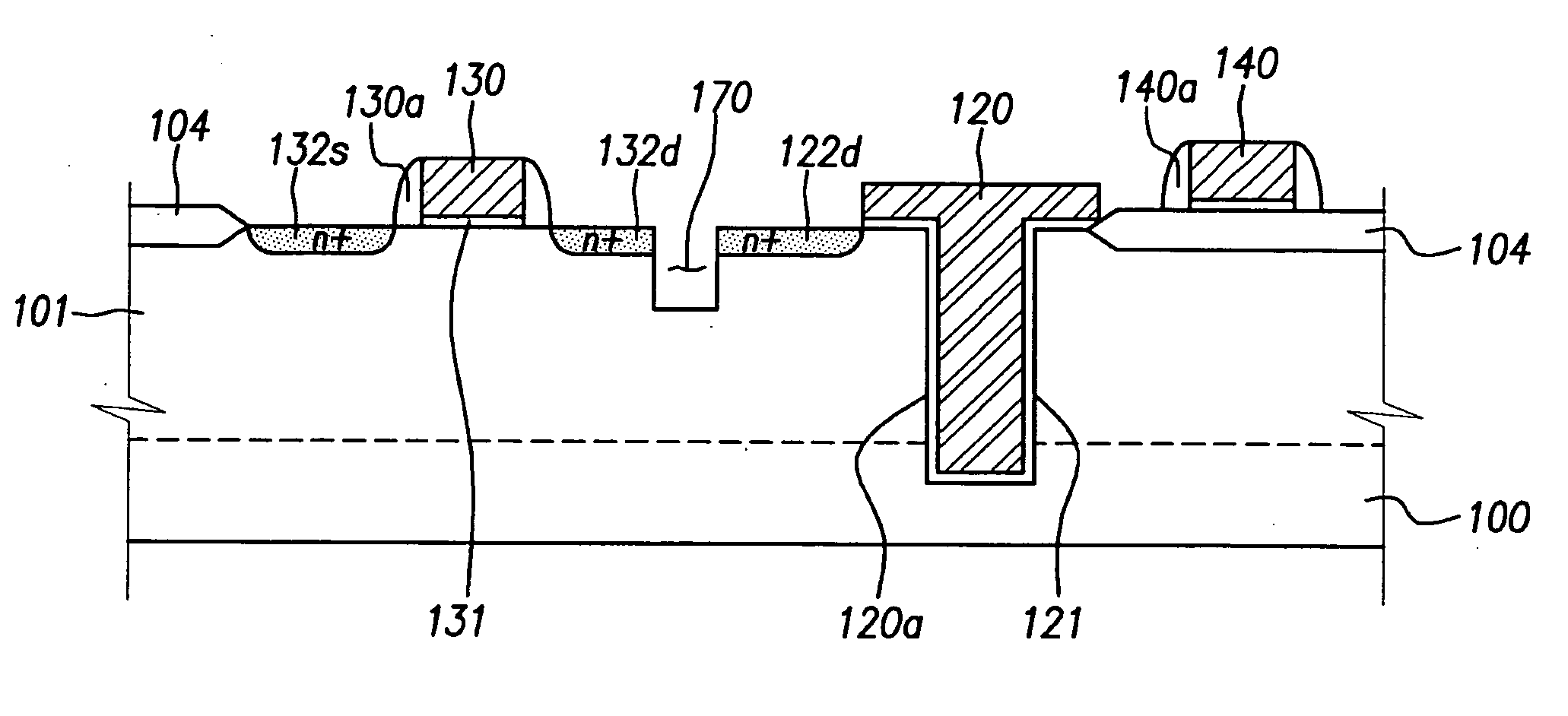
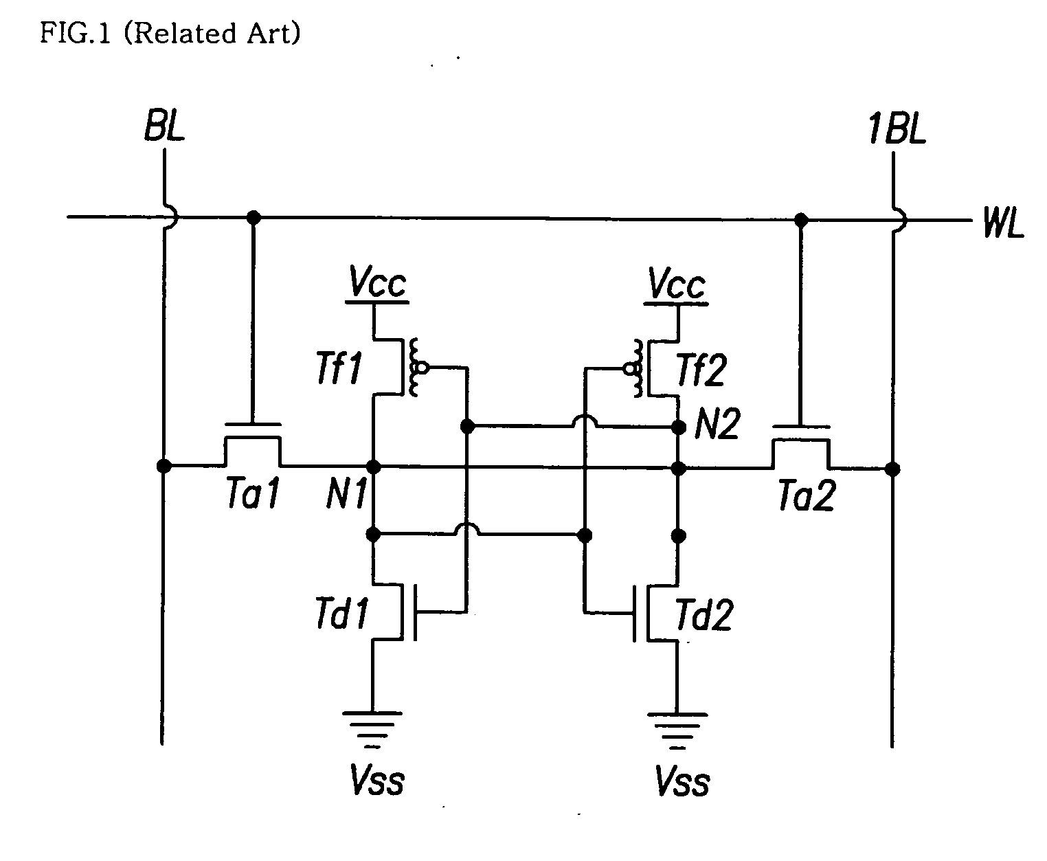
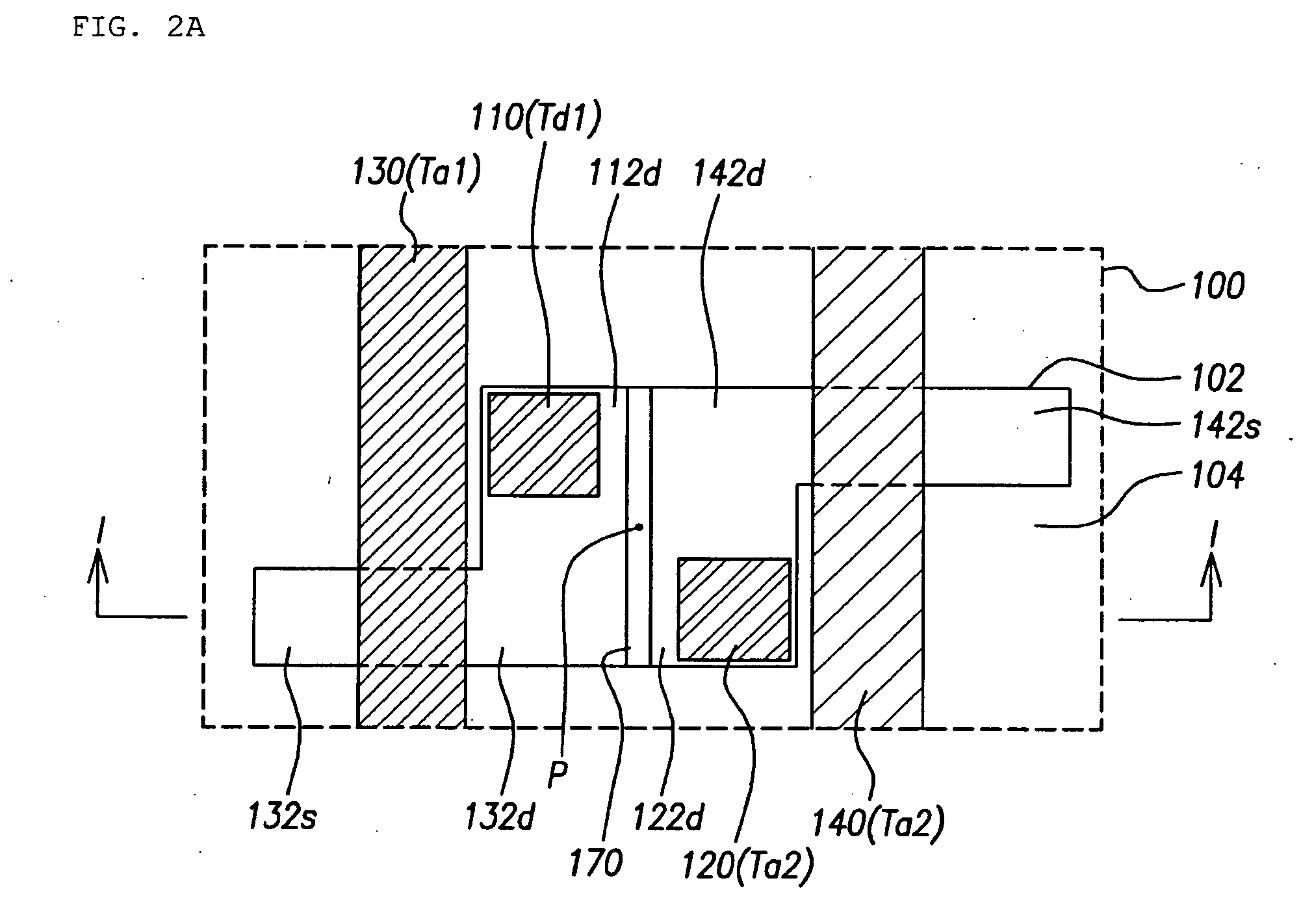
[0023] A circuitry diagram of an SRAM according to the present invention is identical with that of FIG. 1. FIGS. 2A, 3A, and 4A are layout views showing a construction of an SRAM device of the present invention according to a process order. FIGS. 2B, 3B, and 4B are cross-sectional views of the SRAM device taken along line I-I of FIGS. 2A, 3A, and 4A.

[0024] ...


PUM


Abstract

An SRAM device including first and second access transistor composed of an N channel MOS transistor, first and second drive transistors composed of the N channel MOS transistor, and first and second P channel thin film transistor functioning as a pull-up device, comprises: a well formed by implanting a dopant of a conductivity an opposite to that of a semiconductor substrate in the semiconductor substrate; a first active region in which a drain of the first access transistor and a drain of the first drive transistor are formed; a second active region in which a drain of the second access transistor and a drain of the second drive transistor are formed; and a groove line for isolating the first active region and the second active region from each other, wherein the first access transistor, the first drive transistor, the first thin film transistor are formed in point-symmetrical relation with the second access transistor, the second drive transistor, and the second thin film transistor based on a center of the groove line.

Description

BACKGROUND OF THE INVENTION [0001] 1. Field of the Invention [0002] The present invention relates to a static random access memory (referred to as ‘SRAM’ hereinafter) and a method for manufacturing the same. [0003] 2. Description of the Related Art [0004] An SRAM device is a memory device capable of always storing data in a circuit using a latch manner. The SRAM device has high operation speed and low power consumption, and needs not refresh stored information unlike a dynamic random access memory (DRAM) device. [0005] In general, the SRAM device includes two pull-down devices, two access devices, and two pull-up devices. The SRAM device is classified into a complete CMOS type, a high load resistor (HLR) type, and a thin film transistor (TFT) type. In the complete CMOS type SRAM device, a p-channel bulk MOSFET functions as a pull-up device. In the HLR type SRAM device, a poly silicon layer having high resistance value functions as a pull-up device. In the TFT type SRAM device, p-cha...

Claims


Application Information

Patent Timeline
IPC IPC(8): G11C11/00
CPCG11C11/412H01L27/1104H01L27/11H10B10/00H10B10/12
Inventor PARK, SUNG HEE
Owner DONGBU ELECTRONICS CO LTD
Features
  • R&D
  • Intellectual Property
  • Life Sciences
  • Materials
  • Tech Scout
  • Unparalleled Data Quality
  • Higher Quality Content
  • 60% Fewer Hallucinations
Learn More