Design support system of semiconductor integrated circuit, method of designing semiconductor integrated circuit, design support program of semiconductor integrated circuit and method of manufacturing semiconductor integrated circuit

a technology of design support system and integrated circuit, which is applied in the direction of computer aided design, program control, instruments, etc., can solve the problems of poor reliability of electrical connection, deterioration of yield, and difficulty in executing manufacturing process in accordance with design pattern intended in the beginning

Inactive Publication Date: 2007-07-12
KK TOSHIBA
View PDF12 Cites 13 Cited by
  • Summary
  • Abstract
  • Description
  • Claims
  • Application Information

AI Technical Summary

Benefits of technology

[0006] According to an aspect of the invention, there is provided a design support system of a semiconductor integrated circuit includes: a first unit configured to determine a wiring path by calculating wiring resource consuming information for carrying out a connection through a multi-cut via in case that the connection is carried out through the multi-cut via in a wiring region having a plurality of layers; and a second unit configured to replacing a single-cut via into the multi-cut via.
[0007] According to another aspect of the invention, there is provided a method of designing a semiconductor integrated circuit comprising: causing a rough wiring unit to allocate a rough wiring path to a wiring region having a plurality of layers, to estimate the number of vias generated in the rough wiring path, to calculate necessary wiring resource consuming information for carrying out a connection through a multi-cut via in order to provide a detailed wiring based on the rough wiring path, to refer to a wiring congestion degree calculated for each of a plurality of rectangular regions obtained by dividing the wiring region, and to equalize the wiring congestion degree including a provision of the multi-cut via and to assign the rough wiring path, thereby causing a wiring information storing portion to carry out a storage; causing a detailed wiring unit to read the rough wiring path, to provide a detailed wiring in the wiring region by using the wiring resource consuming information, and to store a result of the detailed wiring in the wiring information storing portion; and causing a multi-cut via replacing unit to read the result of the detailed wiring and to replace a via connecting the wiring region with the multi-cut via.
[0008] According to yet another aspect of the invention, there is provided a design support program of a semiconductor integrated circuit for causing a computer to execute: causing a rough wiring unit to allocate a rough wiring path to a wiring region having a plurality of layers, to estimate a number of via generated in the rough wiring path, to calculate necessary wiring resource consuming information for carrying out a connection through a multi-cut via in order to pr

Problems solved by technology

In recent years, a microfabrication of dimensions of a transistor and a wiring which are to be manufactured on a wafer has been advanced and it has been hard to execute a manufacturing process in accordance with a design pattern intended in the beginning.
For this reason, a circuit pattern on a wafer which is actually manufactured is greatly influenced by a factor for a fluctuation in a manufacture, resulting in a poor reliability of an electrical connection so that a deterioration in a yield is caused.
In a technology after the generation of a gate length of 130 nm, p

Method used


Image

  • Design support system of semiconductor integrated circuit, method of designing semiconductor integrated circuit, design support program of semiconductor integrated circuit and method of manufacturing semiconductor integrated circuit
  • Design support system of semiconductor integrated circuit, method of designing semiconductor integrated circuit, design support program of semiconductor integrated circuit and method of manufacturing semiconductor integrated circuit
  • Design support system of semiconductor integrated circuit, method of designing semiconductor integrated circuit, design support program of semiconductor integrated circuit and method of manufacturing semiconductor integrated circuit

Examples


Embodiment Construction

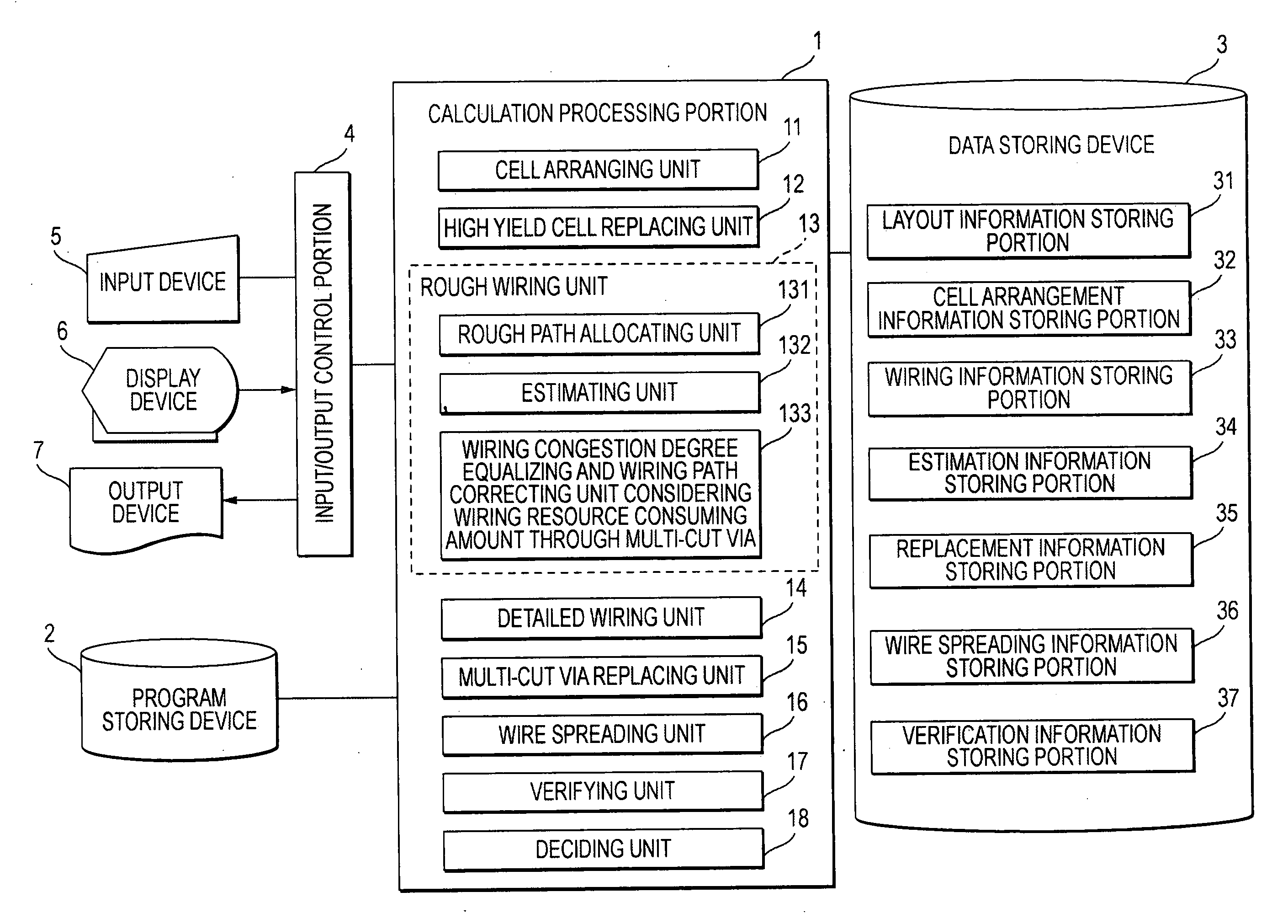
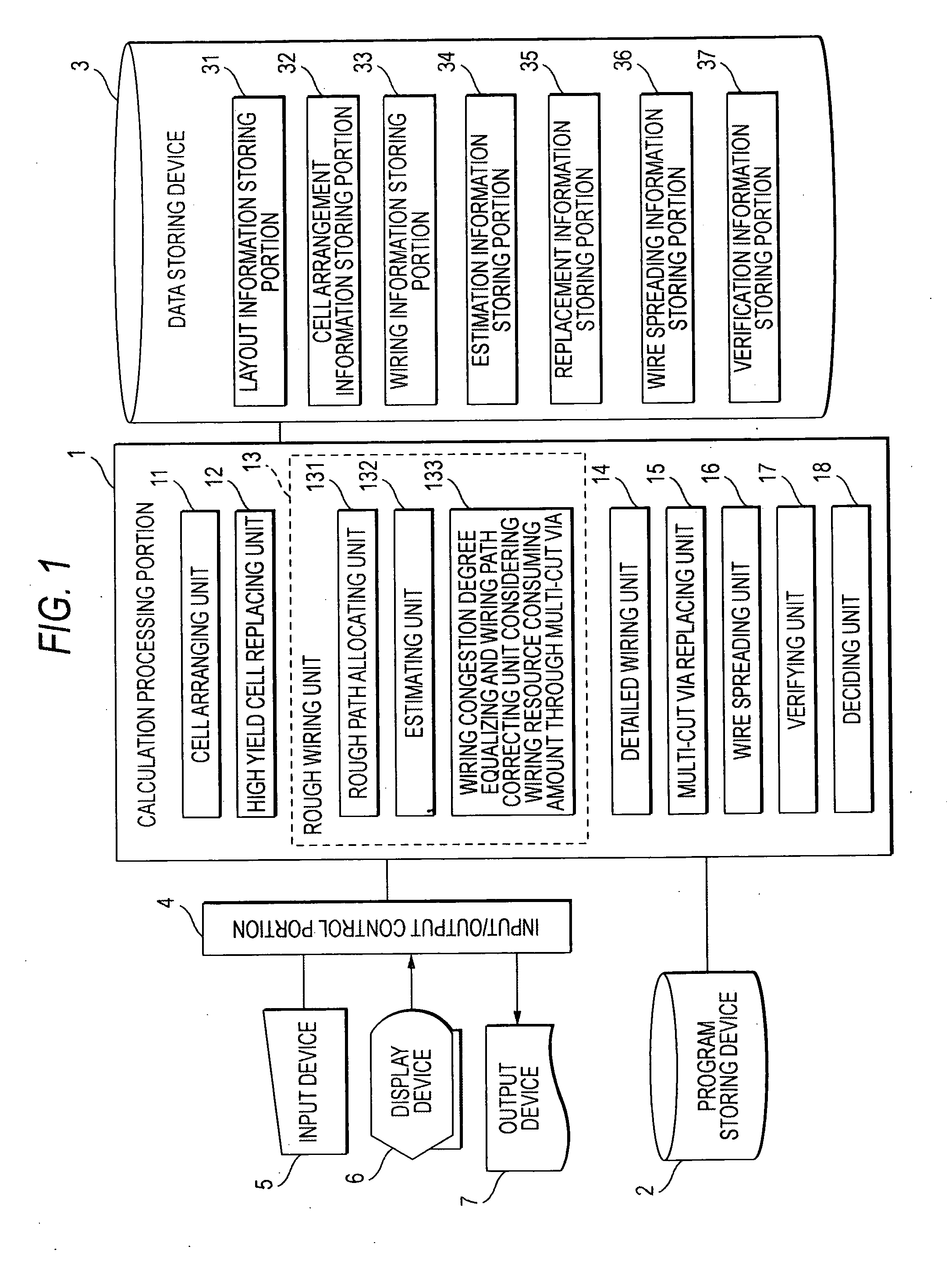
[0010]FIG. 1 is an exemplary block diagram showing an example of a design support system according to an embodiment of the invention.

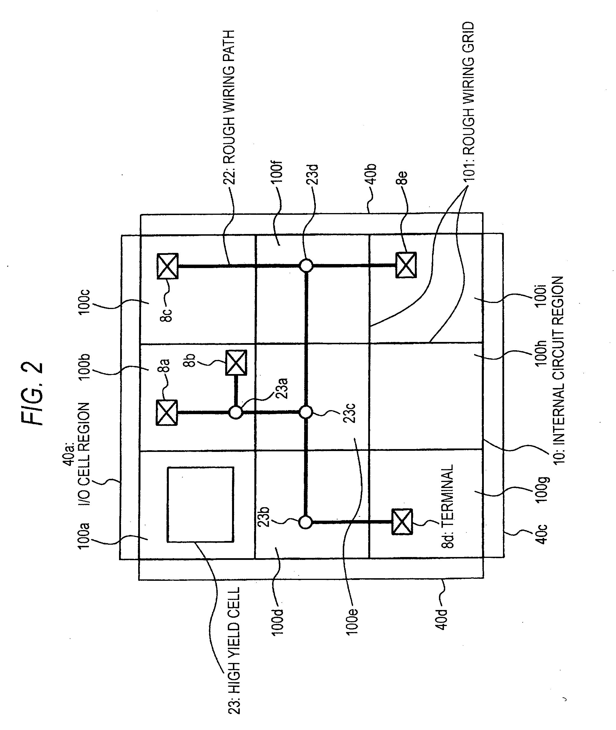
[0011]FIG. 2 is an exemplary diagram showing an example of a layout of a semiconductor integrated circuit according to the embodiment.

[0012]FIG. 3 is an exemplary diagram showing an example of a layout, illustrating a method of designing a semiconductor integrated circuit according to the embodiment.

[0013]FIG. 4 is an exemplary diagram showing an example of the layout, illustrating the method of designing a semiconductor integrated circuit according to the embodiment.

[0014]FIGS. 5A to 5E are explanatory diagram showing a via replacing method of a semiconductor integrated circuit according to the embodiment.

[0015]FIG. 6 is an exemplary flowchart showing the method of designing a semiconductor integrated circuit according to the embodiment.

[0016]FIG. 7 is an exemplary diagram showing a layout, illustrating a comparative example.

[0017]FIG. 8 is an ...


PUM


Abstract

According an aspect of the invention, there is provided a design support system of a semiconductor integrated circuit includes: a first unit configured to determine a wiring path by calculating wiring resource consuming information for carrying out a connection through a multi-cut via in case that the connection is carried out through the multi-cut via in a wiring region having a plurality of layers; and a second unit configured to replacing a single-cut via into the multi-cut via.

Description

CROSS-REFERENCE TO RELATED APPLICATIONS [0001] This application is based on and claims the benefit of priority from the prior Japanese Patent Application No. 2005-360907, filed on Dec. 14, 2005; the entire contents of which are incorporated herein by reference. TECHNICAL FIELD [0002] The present invention relates to a design support system of a semiconductor integrated circuit, a method of designing a semiconductor integrated circuit, a design support program of a semiconductor integrated circuit, and a method of manufacturing a semiconductor integrated circuit. BACKGROUND Description of Related Art [0003] In a design of a semiconductor integrated circuit, a cell or a block which has a logic function and a storing function is disposed in a chip, their input / output terminals are wired respectively and a pattern layout on a chip area is thus determined in order to obtain a desirable circuit operation. A semiconductor integrated circuit using a general gate array method is constituted ...

Claims


Application Information

Patent Timeline
IPC IPC(8): G06F17/50
CPCG06F17/5077G06F30/394
Inventor UEDA, TOSHIAKI
Owner KK TOSHIBA
Why Eureka
Try Eureka