

Charged particle beam apparatus and methods for capturing images using the same
a charge particle and beam technology, applied in the field of charge particle beam apparatus, can solve the problems of reduced measurement reproducibility and instrumental error, and achieve the effect of eliminating instrumental error and reducing the variation of cd valu
- Summary
- Abstract
- Description
- Claims
- Application Information
AI Technical Summary
Benefits of technology
Problems solved by technology
Method used
Image

Examples
modification 1
[Modification 1]
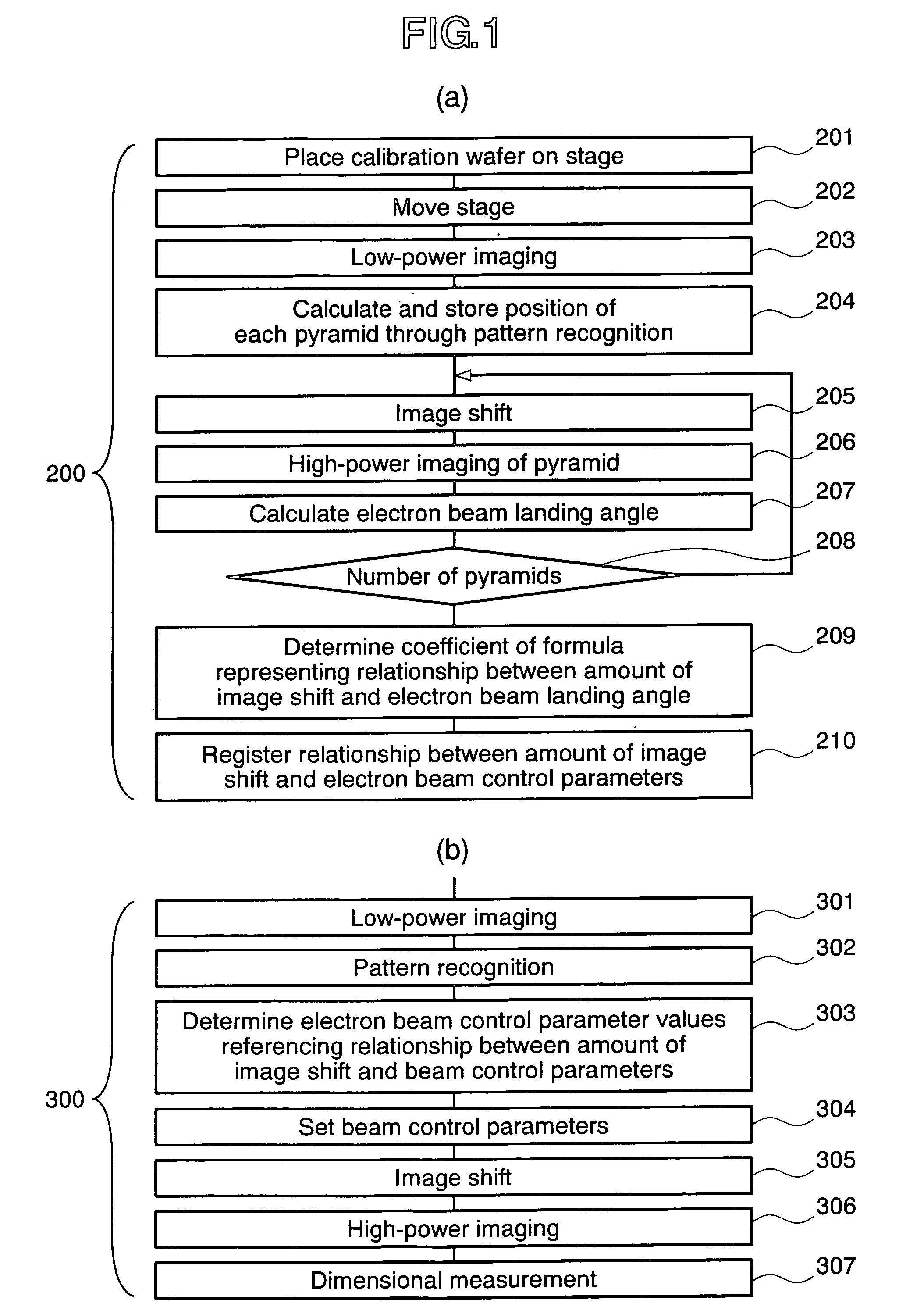
[0055]FIGS. 11A and 11B show a calibration flow chart 200′ and a measurement flow chart 300′ concerning a first Modification, respectively. In the flow charts in FIGS. 11A and 11B, the steps with the same numbers as those in FIG. 1 perform the same processing. In the above-mentioned embodiment, parameters P, Q, dx, and dy in FIG. 5 are obtained in Step 209 in the calibration flow 200. This Modification 1, however, creates a table describing the beam landing angle calculated at the position (x,y) of each pyramid on the viewing field (Step 209′). Then, the present embodiment creates a table describing required beam control parameters (beam incidence conditions for the objective lens, and setup conditions for the focusing lens for correcting the aberration) at each position and then registers these conditions (Step 210′).
[0056]In order to reduce measurement error of the beam landing angle at each position, the obtain beam landing angle φx (i,j) and φy (i,j) at a noticed...
modification 2
[Modification 2]
[0059]FIGS. 12A and 12B show a calibration flow chart 400 and a measurement flow chart 500 concerning Modification 2, respectively. Although the above-mentioned embodiment and Modification 1 intend to make the beam landing angle perpendicular regardless of the amount of image shift, the present embodiment intends to capture inclined images by a predetermined beam landing angle regardless of the amount of image shift. In flow charts in FIGS. 12A and 12B, the steps with the same numbers as those in FIG. 1 perform the same processing.
[0060]In the calibration flow chart 400, Step 401 for setting the beam tilt angle is added prior to Step 203 for capturing low-power images. Also, in the measurement flow chart 500, Step 501 for setting the beam tilt angle is added prior to Step 301 for capturing low-power images. In accordance with the present embodiment, since the beam landing angle becomes a desired tilt angle regardless of the amount of image shift, it is possible to el...
modification 3
[Modification 3]
[0061]The following describes a variation in the polyhedral structure on a sample for beam landing angle calibration.
[0062]In the above-mentioned embodiment, a pyramidal shape produced by the crystal anisotropic etching technology is used as a polyhedral structure on the sample for calibration. A shape which makes it possible to calculate both the electron beam landing angle in the x direction, φx, and the electron beam landing angle in the y direction, φy, by observing a single structure is not limited to a pyramidal shape. For example, as shown in FIG. 15(a), a pyramid with a flat top may be used, which is produced by stopping anisotropic etching halfway. It is possible to obtain a variation in the beam landing angle like a pyramidal shape, for example, by extending line segments 1601 to 1604 in FIG. 15B and obtaining, from the intersection, a virtual apex Q′0 corresponding to the apex Q0 in FIG. 7(b)
[0063]Although FIG. 15A shows an example pyramidal shape with a f...
PUM
 Abstract
Description
Claims
Application Information