Field effect transistor

a field effect transistor and transistor technology, applied in the field of field effect transistors, can solve the problems of difficult control of trade-off, insufficient electric field reduction effect, and inability to achieve simultaneous pursuit of gate breakdown voltage and suppression of collapse, so as to improve the breakdown voltage characteristic, improve the effect of operation at higher voltage and influence on gain reduction

Inactive Publication Date: 2007-07-19
NEC CORP
View PDF7 Cites 37 Cited by
  • Summary
  • Abstract
  • Description
  • Claims
  • Application Information

AI Technical Summary

Benefits of technology

[0017] The object of the present invention is to provide a field effect transistor that can attain simultaneous pursuit of gate breakdown voltage and collapse suppression, which is required to carry out an operation at a higher voltage.
[0019] According to the field effect transistor of the present invention, by arranging the field plate portion, the electric field applied to the end portion of the gate electrode at the side of drain electrode is reduced by the operation of the field plate portion when a high reverse voltage is applied between gate and drain, and therefore the gate breakdown voltage is improved. Further, during the large signal operation, in particular, the surface potential immediately near the gate is effectively modulated by the field plate portion, and therefore collapse in response to the surface trap can be prevented from occurring.
[0020] Moreover, according to the field effect transistor of the present invention, because the thickness of the insulating film in the area near the gate electrode, where the electric field is most concentrated, i.e., the insulating film directly underneath the field plate portion, gradually increases from the gate electrode toward the drain electrode, the film thickness of the insulating film in that area becomes thinner the insulating film in the other area, the electric field concentration is reduced both by operations of the surface negative charges and the field plate portion in this area, and the gate breakdown voltage can be improved. Incidentally, though the surface negative charges cause the collapse, the surface negative charges are generated immediately near the gate electrode and the surface potential can be effectively modulated by field plate portion 5 since the insulating film at the area near the gate electrode is relatively thin. Therefore, the collapse can be suppressed.
[0021] As described above, according to the field effective transistor of the present invention, simultaneous pursuit of the gate breakdown voltage and the collapse suppression can be further excellently attained, and the operation at a higher voltage can be carried out than the conventional one.
[0025] Further, the drain field plate electrode connected to the drain electrode may be arranged on the insulating film between the gate electrode and the drain electrode. According to this arrangement, since the electric field concentration at the end of the drain electrode can be reduced by the drain field plate electrode, the breakdown voltage characteristic can be improved and operation at higher voltage can be performed, in comparison with the arrangement having only the field plate at the side of gate electrode. Also, because the influence on gain lowering is larger in the field plate at the side of gate electrode, the drain field plate electrode is arranged so as to shorten the field plate at the side of gate electrode, whereby the gain can be improved while the breakdown voltage characteristic is maintained.

Problems solved by technology

In such an AlGaN / GaN HJFET, a trade-off exists between the amount of collapse and the gate breakdown voltage, and it is very difficult to control the trade-off.
Therefore, like the conventional art shown in FIG. 3, it is proposed that the field plate portion be arranged between the source electrode and the drain electrode, however, because the thickness of the SiN film directly underneath the field plate portion is thicker, no sufficient electric field reduction effect can be obtained.
In the conventional field plate structure shown in FIG. 3, it is possible to attain simultaneous pursuit of the gate breakdown voltage and the suppression of collapse, which are required at the operating voltage of about 30V, however, it is difficult to attain simultaneous pursuit of the gate breakdown voltage and the suppression of collapse, which are required for the operation at higher voltage, 50V or more.
However, when the size of the field plate exceeds 70% of the interval between the gate electrode and the drain electrode, the gate breakdown voltage is adversely apt to be lowered because the gate breakdown voltage is determined by the electric field concentration to the field plate edge.
Therefore, there is a limit to the effect that collapse suppression can have by increasing the size of the field plate.

Method used


Image

  • Field effect transistor
  • Field effect transistor
  • Field effect transistor

Examples


first embodiment

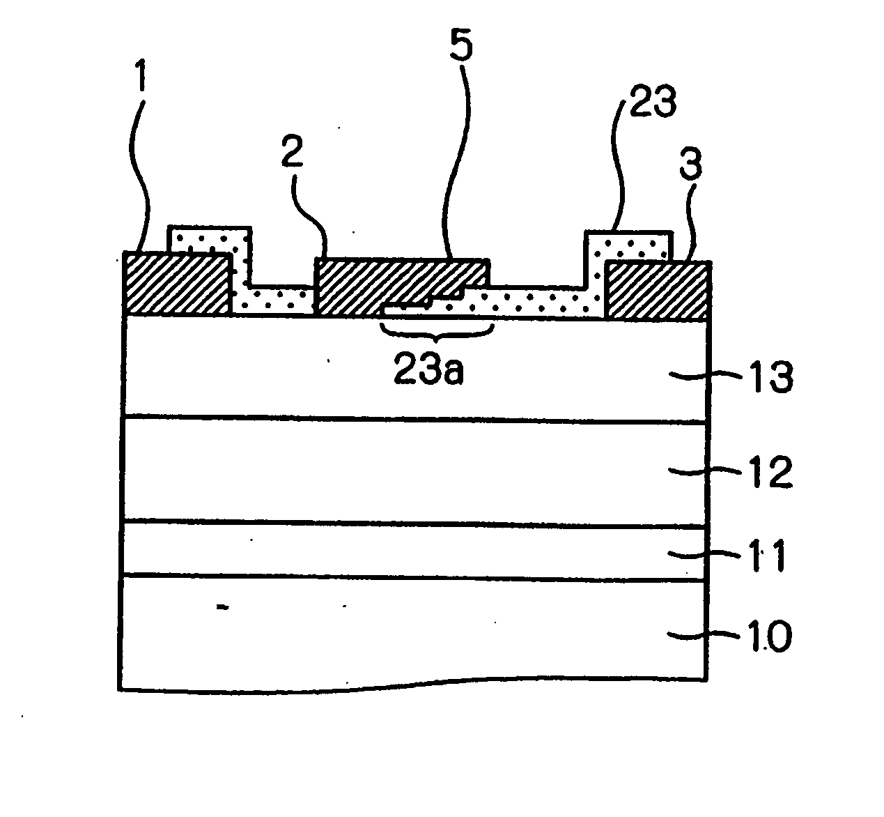
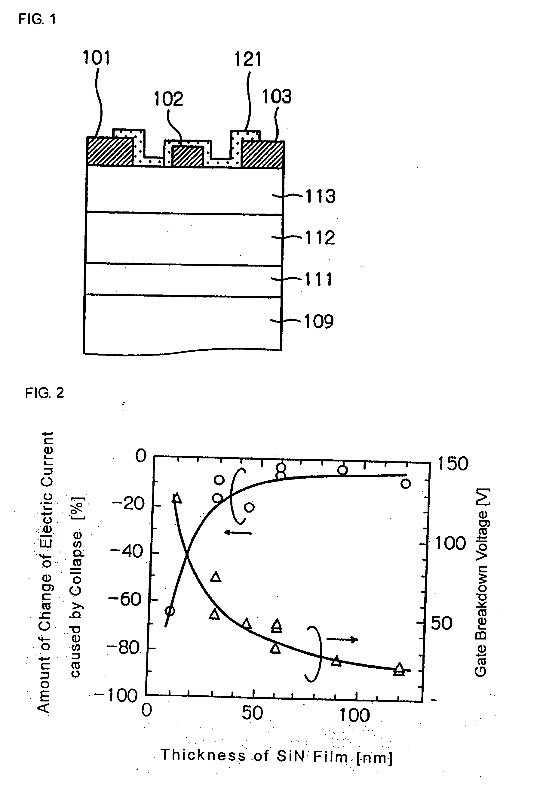
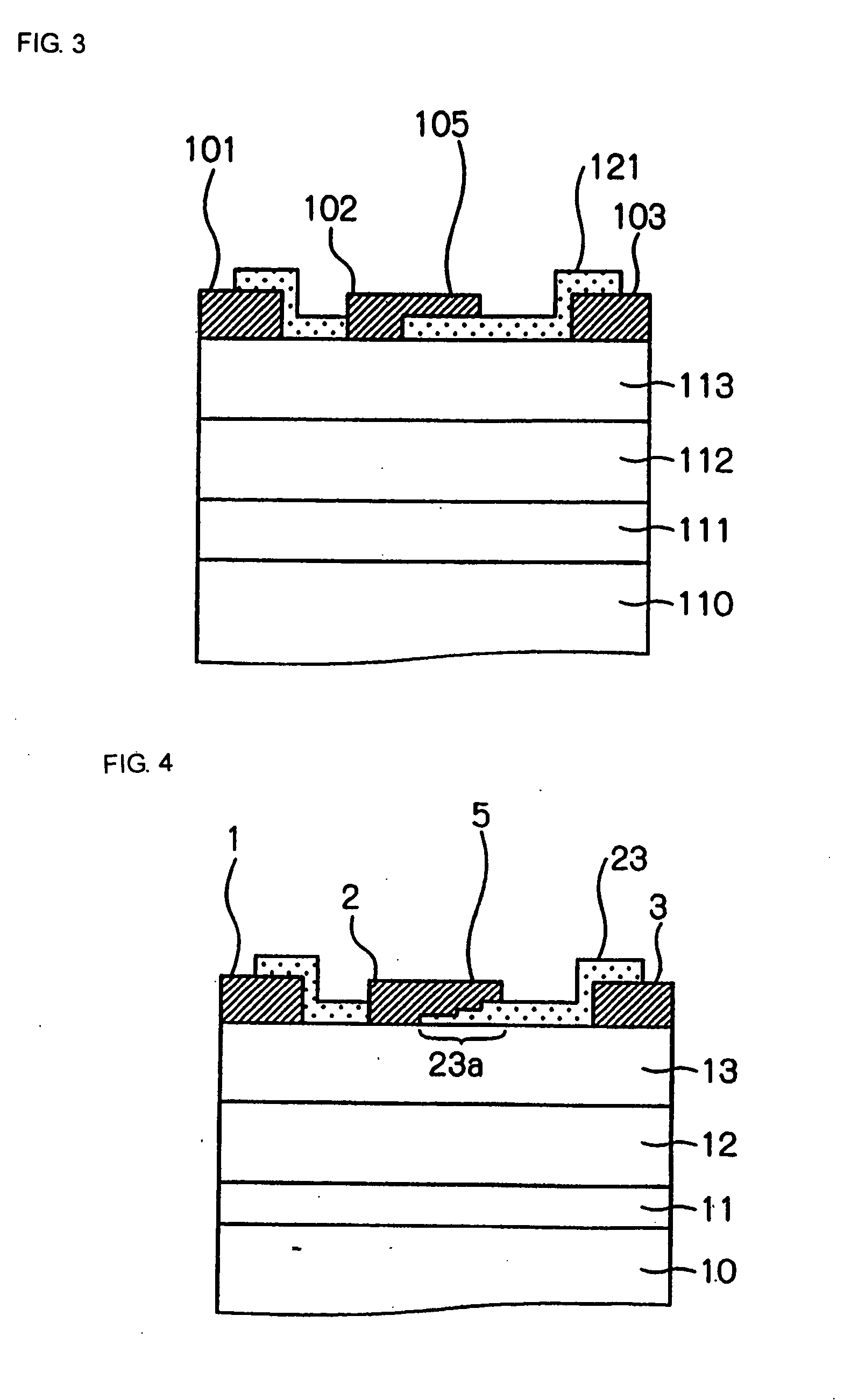
[0037]FIG. 4 is a cross-sectional structure view of a HJFET according to the first embodiment of the present invention.

[0038] The HJFET according to the first embodiment is formed on substrate 10 made of SiC or the like. Buffer layer 11 made of semiconductor is formed on substrate 10. GaN channel layer 12 is formed on buffer layer 11. AlGaN electron supply layer 13 is formed on GaN channel layer 12. Source electrode 1 and drain electrode 3 that are in ohmic contact are arranged on AlGaN electron supply layer 13. Field plate portion 5 that projects toward drain electrode 3 in the form of an eave is arranged between source electrode 1 and drain electrode 3 and gate electrode 2 is arranged in Schottky contact. The surface of AlGaN electron supply layer 13 is covered with SiON film 23, which is an insulating film, and SiON film 23 directly underneath field plate portion 5 (field plate layer 23a) becomes thicker stepwise from gate electrode 2 to drain electrode 3.

[0039] The HJFET of th...

second embodiment

[0049]FIG. 5 is a cross-sectional structure view of a HJFET according to the second embodiment of the present invention.

[0050] The HJFET according to the second embodiment is formed on substrate 10 made of SiC or the like. Buffer layer 11 made of semiconductor is formed on substrate 10. GaN channel layer 12 is formed on buffer layer 11. AlGaN electron supply layer 13 is formed on GaN channel layer 12. Source electrode 1 and drain electrode 3 are arranged on AlGaN electron supply layer 13 in ohmic contact. Between source electrode 1 and drain electrode 3, field plate portion 5 that projects toward drain electrode 3 in the form of an eave is arranged and gate electrode 2 is arranged in Schottky contact. The surface of AlGaN electron supply layer 13 is covered with SiON film 23, which is an insulating film, and SiON film 23 directly underneath field plate portion 5 (field plate layer 23a) becomes thicker continuously from gate electrode 2 to drain electrode 3.

[0051] The HJFET of the ...

third embodiment

[0061]FIG. 7 is a cross-sectional structure view of a HJFET according to the third embodiment of the present invention.

[0062] The HJFET according to the third embodiment is formed on substrate 10 made of SiC or the like. Buffer layer 11 made of a semiconductor is formed on substrate 10. GaN channel layer 12 is formed on buffer layer 11. AlGaN electron supply layer 13 is formed on GaN channel layer 12. Source electrode 1 and drain electrode 3 are arranged on AlGaN electron supply layer 13 in ohmic contact. Between source electrode 1 and drain electrode 3, field plate portion 5 that projects toward drain electrode 3 in the form of an eave is arranged and gate electrode 2 is arranged in Schottky contact. The surface of electron supply layer 13 is covered with SiON film 23, which is an insulating film, and SiON film 23 that is directly underneath field plate portion 5 (field plate layer 23a) becomes thicker continuously from gate electrode 2 to drain electrode 3. Also, drain filed plat...


PUM


Abstract

A field effect transistor includes a semiconductor layer structure including GaN channel layer 12 and AlGa electron supply layer 13, source electrode 1 and drain electrode 3 which are formed on electron supply layer 13 so as to be separated from each other, gate electrode 2 formed between source electrode 1 and drain electrode 3, and SiON film 23 formed on electron supply layer 13. Gate electrode 2 has a field plate portion 5 that projects toward drain electrode 3 in the form of an eave on SiON film 23. The thickness of a portion (field plate layer 23a) of SiON film 23 lying between field plate portion 5 and electron supply layer 13 gradually increases from gate electrode 2 to drain electrode 3.

Description

FIELD EFFECT TRANSISTOR [0001] 1. Technical Field [0002] The present invention relates to a field effect transistor using a III group nitride semiconductor. [0003] 2. Background Art [0004]FIG. 1 is a cross-sectional structure view of a conventional Hetero-Junction Field Effect Transistor (hereinafter, referred to “HJFET”). Such a conventional HJEFT is reported in “Y Ando, 2001, International Electron Device Meeting Digest (IEDM01-381 to 384)”. [0005] In the conventional HJFET shown in FIG. 1, AlN buffer layer 111, GaN channel layer 112, and AlGaN electron supply layer 113 are laminated on sapphire substrate 109 in this order. Also, source electrode 101 and drain electrode 103 are formed on AlGaN electron supply layer 113, and these electrodes 101, 103 are in ohmic contact with AlGaN electron supply layer 113. Further, gate electrode 102 is formed between source electrode 101 and drain electrode 103, and gate electrode 102 is in Schottky contact with AlGaN electron supply layer 113. ...

Claims


Application Information

Patent Timeline
Patent Type & Authority Applications(United States)
IPC IPC(8): H01L29/76H01L21/338H01L29/06H01L29/20H01L29/40H01L29/423H01L29/47H01L29/778H01L29/812H01L29/872
CPCH01L29/2003H01L29/7787H01L29/42316H01L29/402
Inventor OKAMOTO, YASUHIROANDO, YUJIMIYAMOTO, HIRONOBUNAKAYAMA, TATSUOINQUE, TAKASHIKUZUHARA, MASAAKI
Owner NEC CORP
Why Eureka
Try Eureka