Shared-pixel-type image sensors for controlling capacitance of floating diffusion region

a technology of capacitance control and image sensor, which is applied in the field of image sensors, can solve the problems that the image sensor may consume a relatively low amount of power, and achieve the effects of increasing the fill factor, increasing the area of the photoelectric conversion element, and increasing the area

Inactive Publication Date: 2007-07-19
SAMSUNG ELECTRONICS CO LTD
View PDF18 Cites 72 Cited by
  • Summary
  • Abstract
  • Description
  • Claims
  • Application Information

AI Technical Summary

Benefits of technology

[0014]It is therefore a separate feature of an embodiment of a shared-pixel-type image sensor employing one or more aspects of the invention to effectively increase a fill factor

Problems solved by technology

Furthermore, because a MOS image sensor may consume a relatively low amount of power, MOS

Method used


Image

  • Shared-pixel-type image sensors for controlling capacitance of floating diffusion region
  • Shared-pixel-type image sensors for controlling capacitance of floating diffusion region
  • Shared-pixel-type image sensors for controlling capacitance of floating diffusion region

Examples


first embodiment

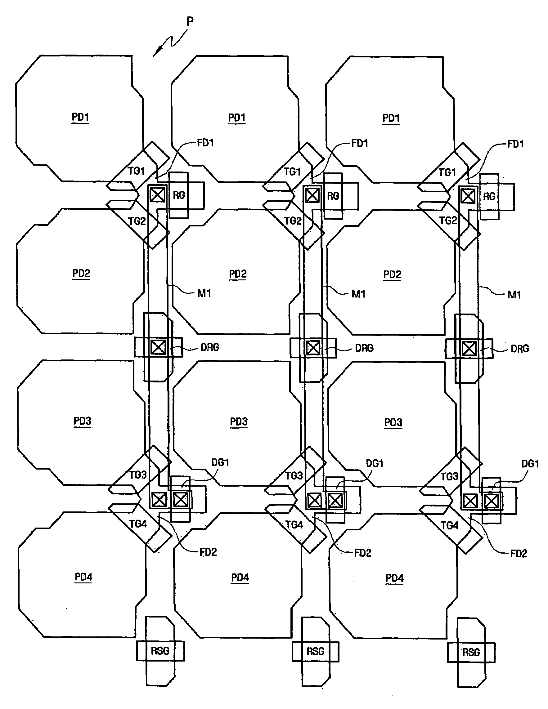
[0065]Referring to FIGS. 3 and 4, the APS array of the image sensor according to the present invention may have the following characteristics. A first active A1 and a second active A2 may be repeatedly arranged. More particularly, pairs of one of the first actives A1 and one of the second active A2 may be repeatedly arranged. Each of the first actives A1 may correspond to a region where two photoelectric conversion elements PD1 and PD2 sharing a first floating diffusion region FD1 may be disposed. Each of the second actives A2 may correspond to a region where two other photoelectric conversion elements PD3 and PD4 sharing a second floating diffusion region FD2 may be disposed.

[0066]Third and fourth actives A3 and A4, which may serve as two independent reading element actives, may be allocated to each pair of first and second actives A1 and A2. That is, in some embodiments of the invention, the first to fourth actives A1, A2, A3, and A4 may form a unit active of one of the 4-shared p...

second embodiment

[0089]Referring to FIG. 5, in each of the 4-shared pixels P, which may be a repeated unit in an APS array of an image sensor according to the present invention, a dummy gate DG2 forming an upper electrode of the MOS capacitor may extend to cover an entire or substantially an entire axis active b of the second active A2.

[0090]That is, in such embodiments of the invention, the MOS capacitor may include a first electrode that may be made of a substrate region of a side adjacent to the second floating diffusion region FD2, and a second electrode that may be made of the gate insulating film laminated on the first electrode, and the dummy gate DG2. The dummy gate DG2 may be disposed on the gate insulating film and may extend to cover the entire or substantially the entire axis active b of the second active A2.

[0091]If the dummy gate DG2 of the MOS capacitor extends to cover the entire axis active b of the second active A2, a capacitance may be proportional to areas of the upper and lower ...

third embodiment

[0094]In the 4-shared pixels P that may be repeated unit in an APS array of an image sensor according to the present invention, a first active A1′ and a second active A2′ form the unit active of the 4-shared pixel P.

[0095]In the 4-shared pixel P, two photoelectric conversion elements PD1 and PD2, the first floating diffusion region FD1, and the plurality of reading elements may be disposed in the first active A1′. The other two photoelectric conversion elements PD3 and PD4, the second floating diffusion region FD2, and the MOS capacitor may be formed in the second active A2′. Each of the first active A1′ and the second active A2′ may correspond to a one-axis-merged dual lobe-typed active.

[0096]That is, in each of the first active A1′ and the second active A2′, the dual lobe actives a may be merged with one axis active b′ by a connection active c. In this case, the dual lobe active a of the first active A1 may correspond to a dual photoelectric conversion element active where the two...


PUM


Abstract

A shared-pixel-type image sensor includes a semiconductor substrate, four photoelectric conversion elements disposed adjacent to one another in one direction on the semiconductor substrate, two first transmission elements transmitting charges accumulated in two adjacent ones of the photoelectric conversion elements to a first floating diffusion region, respectively, two second transmission elements transmitting charges accumulated in the other two adjacent photoelectric conversion elements to a second floating diffusion region electrically coupled with the first floating diffusion region, respectively, MOS capacitors that are electrically coupled with the first or second floating diffusion region, a reset element resetting the charges of the first and second floating diffusion regions to a reference value, and a drive element and an select element outputting the charges of the first or second floating diffusion region.

Description

BACKGROUND OF THE INVENTION[0001]1. Field of the Invention[0002]The present invention relates to image sensors. More particularly, the invention relates to shared-pixel-type image sensors for controlling the capacitance of a floating diffusion region.[0003]2. Description of the Related Art[0004]An image sensor converts optical images into electronic signals. With advancements made in computers and communication devices, demand for image sensors having improved performance characteristics has increased in various fields, e.g. digital cameras, camcorders, personal communication systems (PCSs), game machines, security cameras, medical micro cameras, robots, or the like.[0005]A MOS image sensor may have a simple driving method and may be implemented by various scanning methods. In MOS image sensors, a signal processing circuit may be integrated in one chip, and thus a size of a product including such a MOS image sensor can be reduced. Further, MOS image sensors are generally compatible ...

Claims


Application Information

Patent Timeline
IPC IPC(8): H01L31/113H01L27/146H04N5/335H04N5/369H04N5/374
CPCH01L27/14603H01L27/14641H04N5/335H01L27/14609H04N25/00H01L27/146
Inventor PAIK, KEE-HYUNLEE, SEOK-HALEE, KANG-BOK
Owner SAMSUNG ELECTRONICS CO LTD
Why Eureka
Try Eureka