
MOS transistor with elevated source and drain structures and method of fabrication thereof

a technology of source and drain structure and mos transistor, which is applied in the direction of transistors, electrical devices, semiconductor devices, etc., can solve the problems of short channel effect, impact on switching performance, and general phenomenon of scaled-down mos transistor, and achieve the effect of increasing the effective channel length and limiting the diffusion of dopan

Inactive Publication Date: 2007-07-19
SAMSUNG ELECTRONICS CO LTD
View PDF31 Cites 6 Cited by
  • Summary
  • Abstract
  • Description
  • Claims
  • Application Information

AI Technical Summary

Benefits of technology

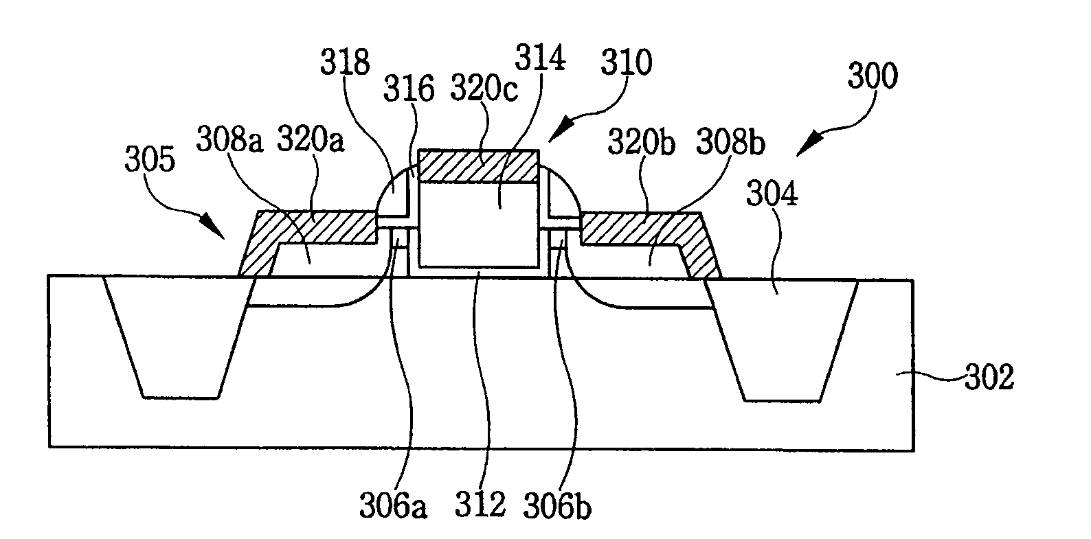
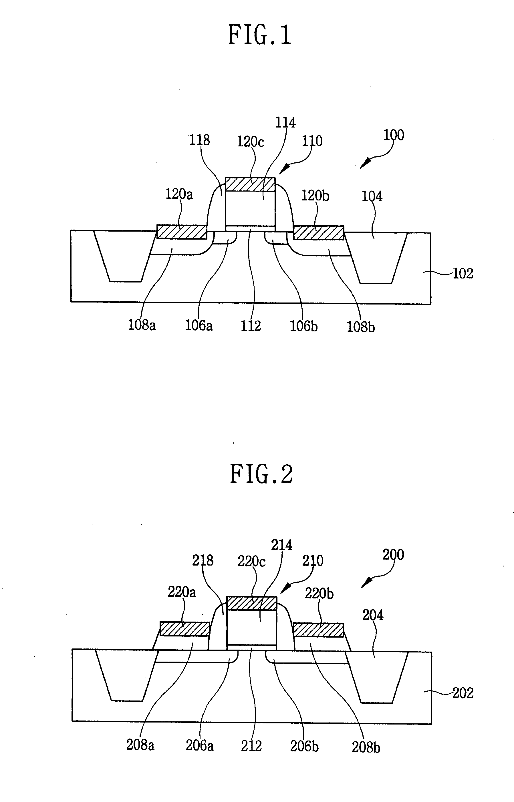
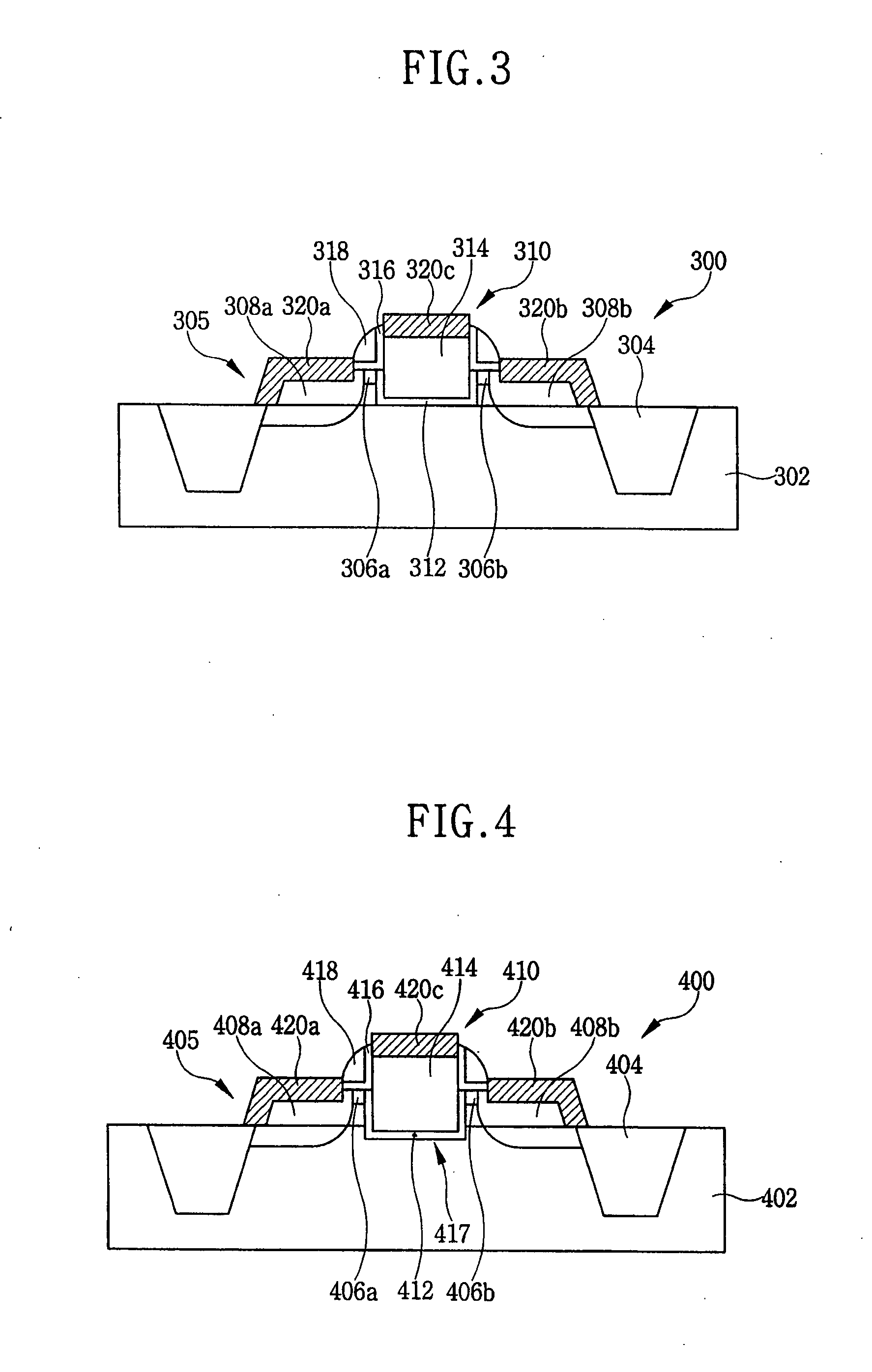
[0008] The present invention is directed to a MOS transistor having elevated source and drain structures, and a method of formation thereof, that overcomes the limitations of the conventional embodiments. In particular, the present invention provides for a transistor that includes source and drain extension regions in which the diffusion of dopants into the channel region is mitigated or eliminated. This is accomplished, in part, by elevating the source and drain extension regions into the epitaxial layer formed on the underlying substrate. In doing so, the effective channel length is increased, while limiting dopant diffusion into the channel region.
[0009] The performance characteristics of the transistor of the present invention can be accurately determined by controlling the respective geometries (i.e. depths and widths) of the source / drain extension regions, the source / drain regions, the channel width and an optional trench formed in the underlying substrate. In the various embodiments, the source / drain regions and the source / drain extension regions may extend partially, or fully, through the epitaxial layer, or even into the underlying semiconductor substrate.

Problems solved by technology

However, scaled-down MOS transistors generally suffer from a phenomenon referred to as the “short-channel effect”.
The short-channel effect has an adverse impact on the switching performance of the transistors, because such switching is inefficiently controlled by the gate electrode, which leads to an undesired decrease in the threshold voltage.
A problem lies in that impurities in the source / drain extension regions 106a / 106b tend to diffuse to the region immediately under the gate 110.
This inhibits the flow of electric current, thus decreasing operation speed.
A second problem concerns the rise of channel dopant concentration, which in turn causes a rise in threshold voltage in the field effect transistor.
For this reason, any rise in the threshold voltage of MOS transistor due to the rise in channel dopant concentration is undesirable.
On the other hand, a channel doping level that is too high in scaled-down devices gives rise to superfluous leakage current and junction breakdown.

Method used


Image

  • MOS transistor with elevated source and drain structures and method of fabrication thereof
  • MOS transistor with elevated source and drain structures and method of fabrication thereof
  • MOS transistor with elevated source and drain structures and method of fabrication thereof

Examples


second embodiment

[0063] A second embodiment of the invention is shown and described above with reference to FIG. 4. In the second embodiment, the gate electrode 414 is formed in a trench or a recessed portion 417 of the semiconductor substrate 402. Other components of the transistor configuration of the second embodiment are similar to those of the first configuration above, and therefore their description will be omitted here. Components of FIG. 4 having a reference numeral beginning with the prefix “4” and a unique suffix “4xx” share the same purpose as those components of FIG. 3, described above, having the same suffix “3xx”.

[0064] A method of fabricating a semiconductor device according to the second embodiment of the present invention will now be described with reference to FIGS. 10A-10C.

[0065] The processes preceding the step shown at FIG. 10A are identical to those shown in FIGS. 9A-9D above with reference to the first embodiment.

[0066] Referring to FIG. 10A, the dummy gate, including the ...


PUM


Abstract

A transistor and method of formation thereof includes source and drain extension regions in which the diffusion of dopants into the channel region is mitigated or eliminated. This is accomplished, in part, by elevating the source and drain extension regions into the epitaxial layer formed on the underlying substrate. In doing so, the effective channel length is increased, while limiting dopant diffusion into the channel region. In this manner, performance characteristics of the transistor can be accurately determined by controlling the respective geometries (i.e. depths and widths) of the source / drain extension regions, the source / drain regions, the channel width and an optional trench formed in the underlying substrate. In the various embodiments, the source / drain regions and the source / drain extension regions may extend partially, or fully, through the epitaxial layer, or even into the underlying semiconductor substrate.

Description

RELATED APPLICATIONS [0001] This application is a divisional of U.S. application Ser. No. 10 / 697,826, filed on Oct. 30, 2003, which relies for priority upon Korean Patent Application No. 03-12793, filed on Feb. 28, 2003, the contents of which are herein incorporated by reference in their entirety.BACKGROUND OF INVENTION [0002] In the semiconductor industry, minimization of the feature size of MOS transistors in integrated circuits is a common goal. This goal is essentially driven by the need to produce integrated circuits at ever-lower costs, while improving circuit functionality and speed. Such downscaling can be achieved by reducing the characteristic dimensions of the transistors, i.e. reducing the gate lengths, the gate oxide thickness, and the junction depths, and by increasing the channel doping levels. However, scaled-down MOS transistors generally suffer from a phenomenon referred to as the “short-channel effect”. The short-channel effect has an adverse impact on the switchi...

Claims


Application Information

Patent Timeline
Patent Type & Authority Applications(United States)
IPC IPC(8): H01L29/76H01L21/28H01L21/336H01L29/417H01L29/423H01L29/49H01L29/78H01L29/786
CPCH01L29/665H01L29/66545H01L29/7834H01L29/66628H01L29/66621H01L29/78
Inventor KO, YOUNG-GUNOH, CHANG-BONG
Owner SAMSUNG ELECTRONICS CO LTD
Learn More