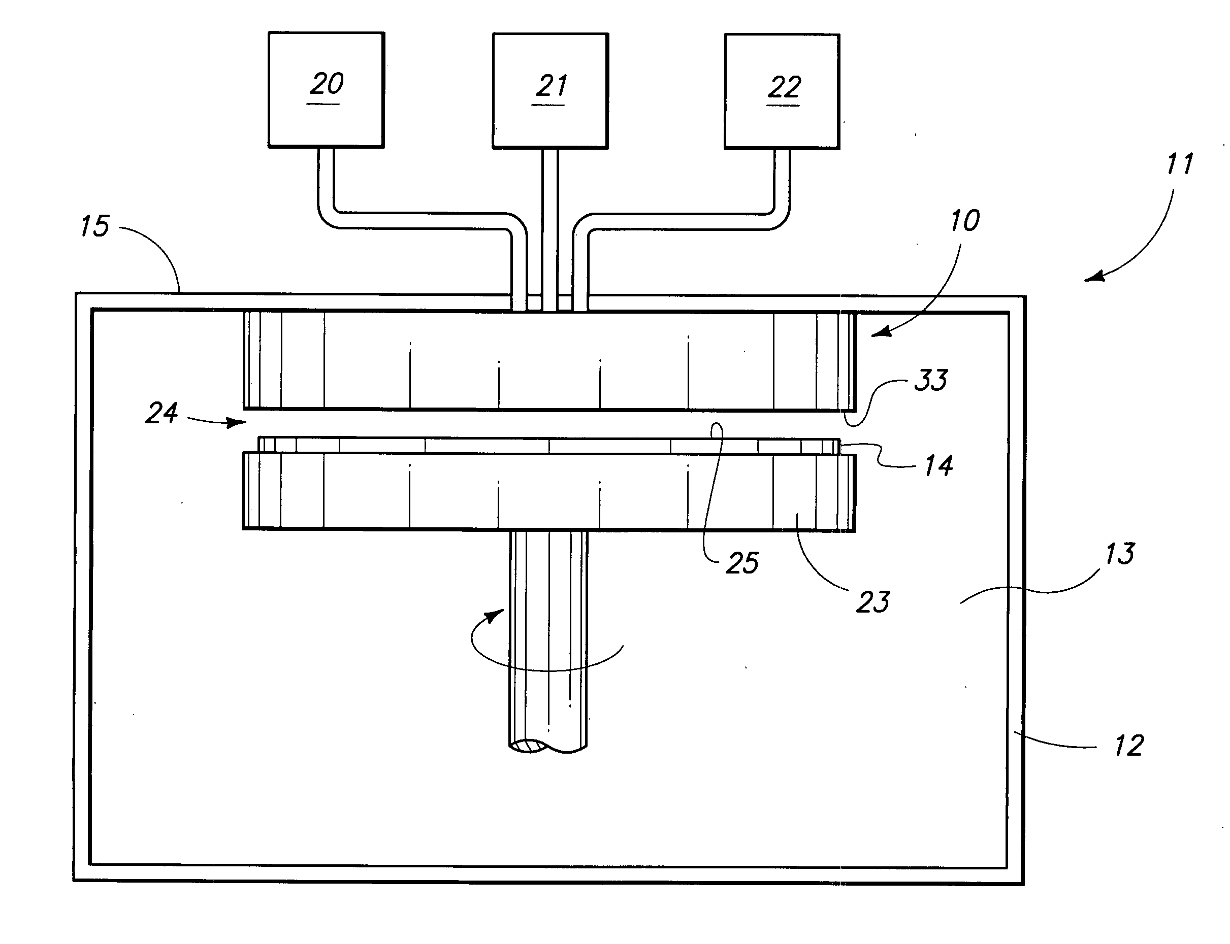
[0006] A first aspect of the present invention relates to an assembly for delivering a reactant material to a substrate which includes a delivery member which has a first surface, and an opposite second surface, and wherein the second surface is positioned adjacent to a substrate, and wherein an elongated substantially continuous channel is formed in the second surface of the delivery member, and which is coupled in fluid flowing relation relative to a source of the reactant material, and wherein the elongated substantially continuous channel delivers the reactant material to the substrate.
[0007] Still another aspect of the present invention relates to an assembly for delivering a reactant material to a substrate, and which includes a pedestal which rotatably supports a substrate in a substantially
horizontal orientation; and a delivery member having a main body which is defined by a
central region, and a
peripheral edge, and wherein the delivery member defines a plurality of elongated reactant delivery channels which each have a first end which is located in the
central region of the delivery member, and which are each coupled with a source of reactant material, and an opposite second end which is located near the
peripheral edge of the main body, and wherein the respective reactant delivery channels are dimensioned so as to deliver a variable amount of the respective reactant materials along the length of the respective reactant delivery channels, and wherein the plurality of reactant delivery channels are located in proximity to each other so as to facilitate the
chemical reaction of the respective reactant materials to form a product which is delivered in a substantially uniform fashion to a surface of the rotating substrate.
[0008] Still another aspect of the present invention relates to an assembly for delivering a reactant material to a rotating substrate which includes a plurality of reactant materials which when chemically reacted together form a resulting product which is delivered to a surface of a rotating substrate; and a delivery member coupled in fluid flowing relation relative to the respective reactant materials, and positioned above the rotating substrate, and wherein the delivery member delivers the respective reactant materials into a
chemical reaction zone which is located therebetween the delivery member and the rotating substrate, and in a manner where the resulting product is chemically produced in the
chemical reaction zone following the release of the reactant materials from the delivery member, and wherein the delivery member is arranged so as to deliver a variable amount of reactant materials which results in the generation of an amount of the resulting product which is correlated to the speed of rotation of a region of the rotating substrate which is positioned therebeneath the delivery member to cause a substantially uniform deposition of the resulting product on the surface of the rotating substrate.
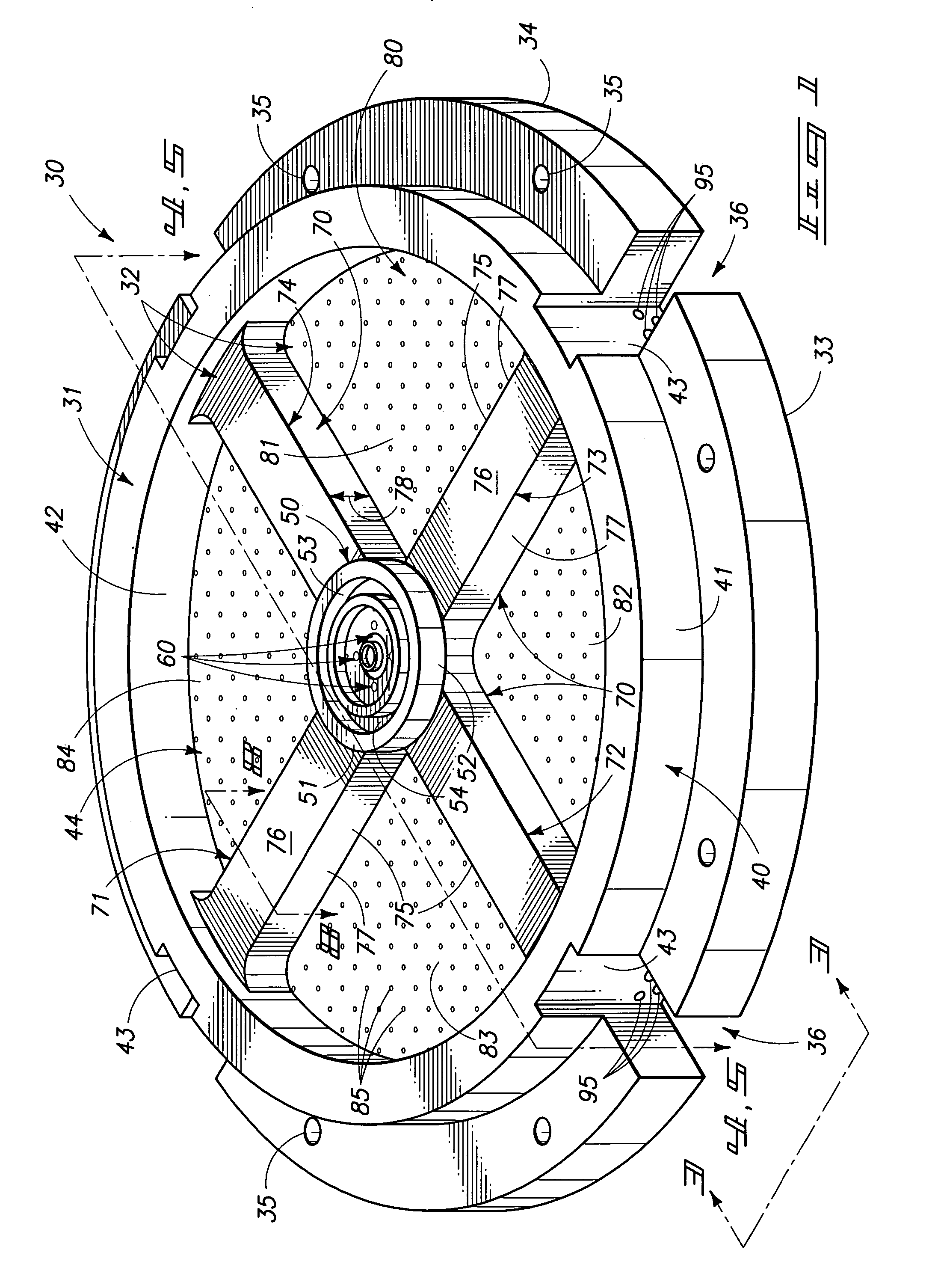
[0009] A further aspect of the present invention relates to an assembly for delivering a reactant material to a substrate which includes a fluid delivery member having a main body defined by a first surface, an opposite second surface, and a
peripheral edge, and wherein the first surface defines a substantially centrally disposed reactant delivery region which is coupled in fluid flowing relation relative to a plurality of reactants which are to be delivered by the fluid delivery member to a chemical
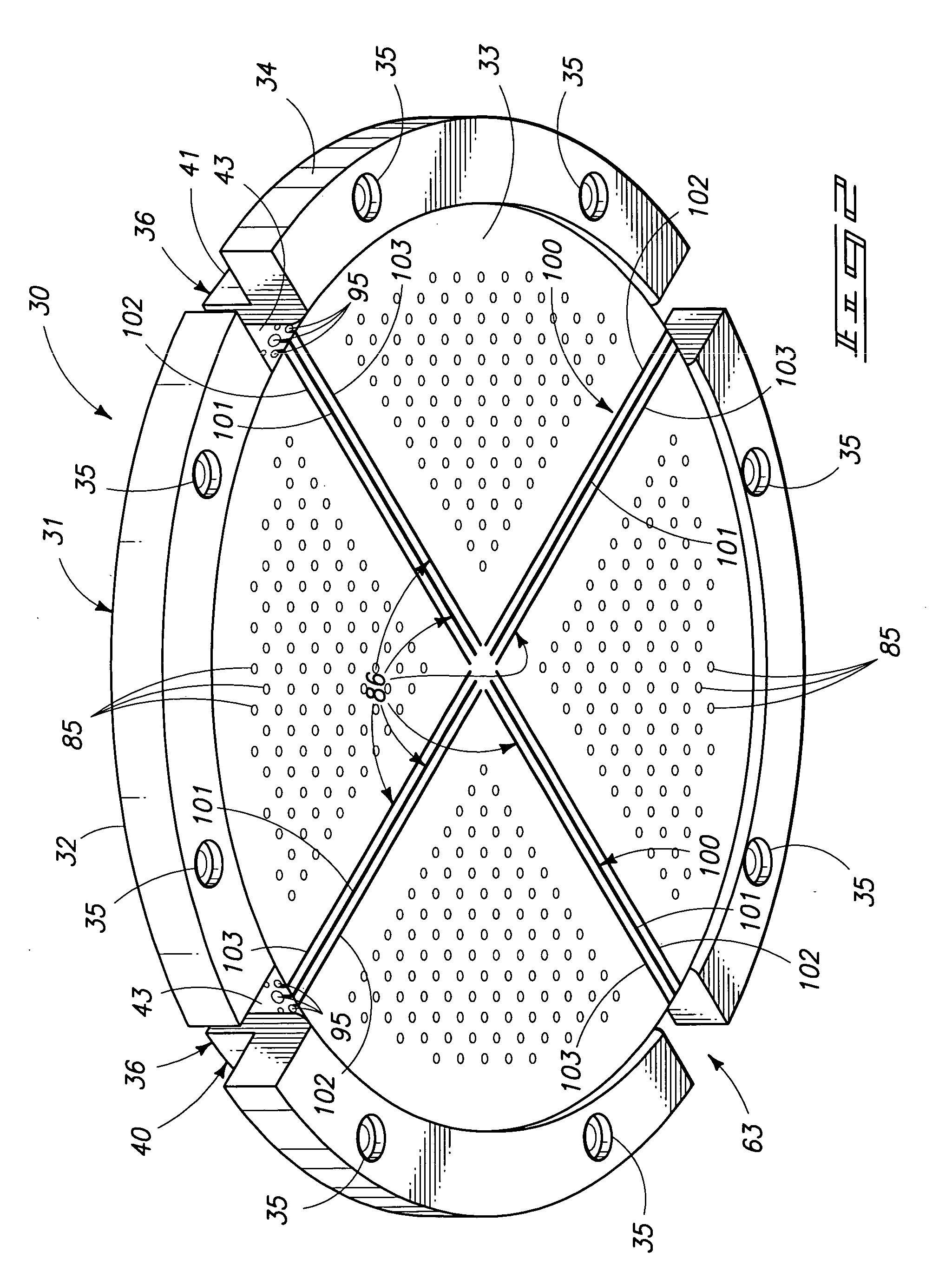
reaction zone which is located adjacent to the second surface of the fluid delivery member, and wherein the first surface is further defined by a plurality of structural members which extend radially outwardly relative to the centrally disposed reactant delivery region to the peripheral edge of the main body, and wherein a plurality of passageways are formed in the intermediate regions and which facilitate the passage of a source of gas therethrough, and wherein a fluid distribution passageway is formed in each of the plurality of structural members, and wherein the fluid distribution passageway has a first end which is coupled in fluid flowing relation relative the centrally disposed reactant delivery region, and an opposite second end which is located near the peripheral edge, and wherein the fluid distribution passageway extends in an acutely angulated orientation therebetween the centrally disposed reactant delivery region, and the peripheral edge, and wherein the first end of the fluid distribution passageway is located near the first surface of the main body, and the second end of the fluid distribution passageway is located near the second surface thereof, and wherein an elongated slot having a variable depth, is formed in the second surface of the main body, and which individually couples the fluid distribution passageway in fluid communication with the second surface, and wherein the elongated slot has a
depth dimension which diminishes when measured from the first end of the fluid distribution passageway, in the direction of the second end of the fluid distribution passageway, and wherein reactants delivered to the centrally disposed reactant delivery region pass into the first end of the fluid distribution passageway, and then through the elongated slot, for subsequent delivery into the chemical reaction region which is located adjacent to the second surface.
[0011] Another aspect of the present invention relates to an assembly for delivering a reactant material to a substrate, and which includes a delivery member having opposite first and second surfaces, and wherein the second surface is positioned adjacent to a substrate, and wherein a substantially continuous fluid distribution passageway is formed in the delivery member and is further coupled in fluid flowing relation relative to a source of reactant material, and wherein a plurality of reactant delivery passageways are formed in the second surface and extend in the direction of the first surface, and which are coupled in fluid flowing relation relative to the substantially continuous fluid distribution passageway, and wherein the respective reactant delivery passageways deliver the reactant material in amounts which facilitate a deposit of a substantially uniform amount of the reactant material on the adjacent substrate.
[0006] A first aspect of the present invention relates to an assembly for delivering a reactant material to a substrate which includes a delivery member which has a first surface, and an opposite second surface, and wherein the second surface is positioned adjacent to a substrate, and wherein an elongated substantially continuous channel is formed in the second surface of the delivery member, and which is coupled in fluid flowing relation relative to a source of the reactant material, and wherein the elongated substantially continuous channel delivers the reactant material to the substrate.

