Check patentability & draft patents in minutes with Patsnap Eureka AI!

High voltage tolerant output buffer

a high voltage tolerance and output buffer technology, applied in the field of output buffers, can solve the problems of substrate current flow, gate oxide of both pmos and nmos may break down, etc., and achieve the effect of high voltage tolerance output buffer, less power dissipation, and high voltage output buffer

Active Publication Date: 2007-07-26
STMICROELECTRONICS PVT LTD
View PDF4 Cites 5 Cited by
  • Summary
  • Abstract
  • Description
  • Claims
  • Application Information

AI Technical Summary

Benefits of technology

[0012] An object of the present invention is to provide a high voltage tolerance output buffer in an IC package that dissipates less power. It is another object of the present invention to provide a high voltage output buffer that uses less hardware and is hence cost advantageous.

Problems solved by technology

The problem associated with this type of operation is that tristate buffer operating at 3.3 volts may not be able to tolerate a 5 volts voltage level.
This results in substrate current flow.
Moreover, if the voltage across any transistor increases beyond a critical limit, the gate oxide of both PMOS and NMOS may break down.
However, the circuit faces one problem.
However, this is not desired.
As a result, the inverter dissipates power.

Method used


Image

  • High voltage tolerant output buffer
  • High voltage tolerant output buffer
  • High voltage tolerant output buffer

Examples


Embodiment Construction

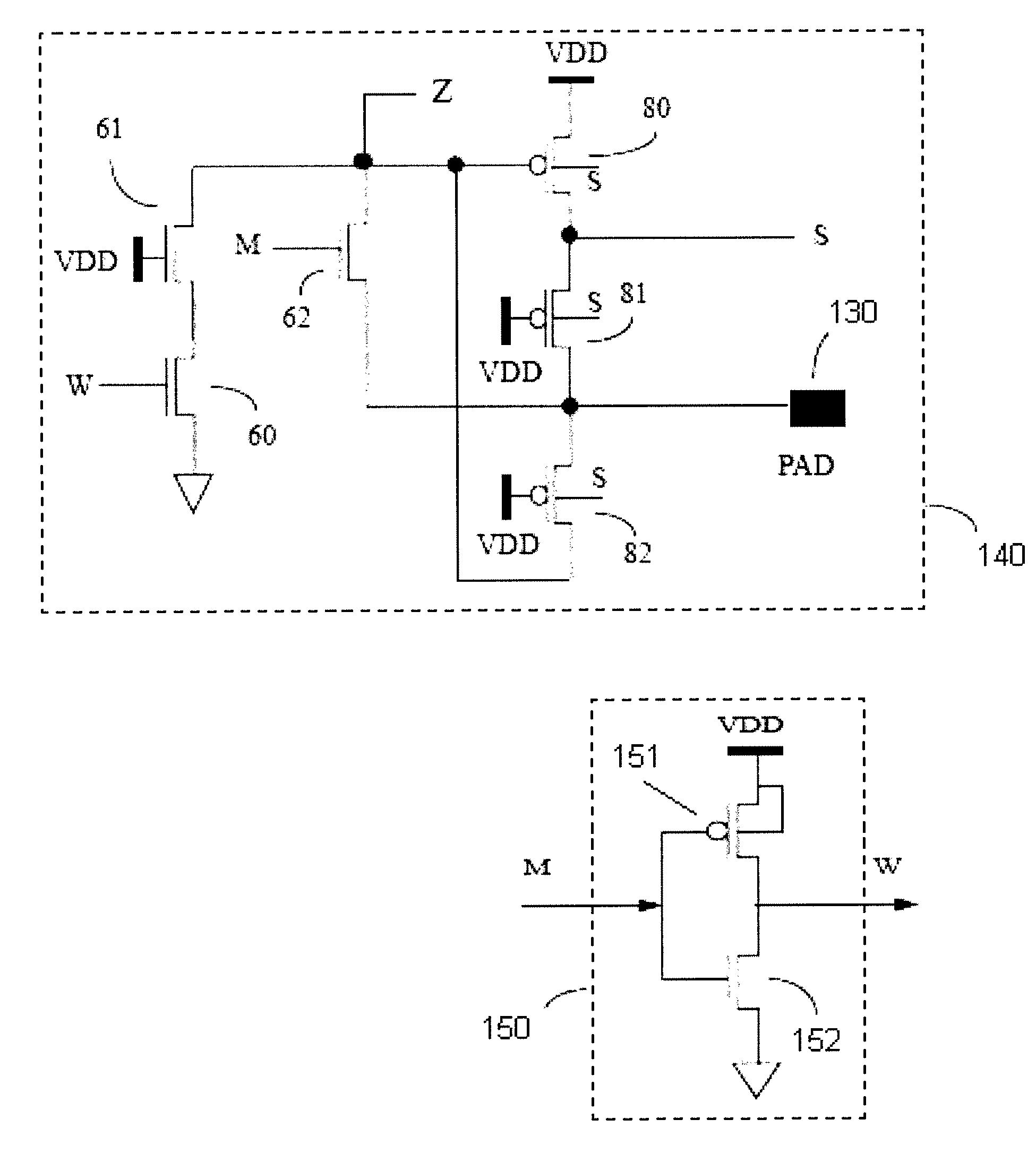
[0026] The circuit for generating substrate voltage (140) is shown in FIG. 3. It comprises of three NMOSs (60), (61) and (62) and three PMOSs (80), (81) and (82). The source of (60) is connected to ground while its gate is connected to W. The drain of (60) is connected to one of the terminals of (61) while the gate of (61) is connected to VDD. The second terminal of (61) is connected to node Z, the gate of (80). The NMOS (62) is connected between PAD (130) and Z. (80) is connected in between VDD and substrate voltage terminal S. (81) is connected between S and PAD (130). The gate of (81) is connected to VDD. The PMOS (82) is connected between PAD (130) and the gate of (80). The gate of (82) is connected to VDD and the bulk of (80), (81) and (82) are connected to S. The inverter (150) is also shown in FIG. 3. It comprises of PMOS (151) and NMOS (152). The drains of (151) and (152) are connected to W. The source and bulk of both (151) and (152) are connected to VDD and ground respecti...


PUM


Abstract

A high voltage tolerant output buffer uses a substrate voltage control circuit to control the voltage at the substrate of the transistors in the output buffer. The circuitry of output buffer is such that the voltage between any two terminals of any of the transistors is not allowed to exceed the supply voltage of the output buffer. At the same time, the voltage at the source or drain of transistors of output buffer is not allowed to increase beyond its substrate voltage. The proposed circuit for output buffer can tolerate voltages higher than the voltage at which it is operated. The novel circuitry uses less hardware and prevents power dissipation in the circuit.

Description

RELATED APPLICATION [0001] This application claims priority of India Patent Application No. 3473 / Del / 2005 filed Dec. 26, 2005, which is incorporated herein in its entirety by this reference. FIELD OF THE INVENTION [0002] The present invention relates to the field of I / O buffers for integrated circuits, and more particularly to an output buffer capable of tolerating high voltages. BACKGROUND OF THE INVENTION [0003] An integrated circuit (IC) package has a number of components present on a single chip to perform a specific function. Apart from the basic circuitry, each IC package has a I / O block associated with it. The function of this I / O block is to interface with other IC packages or electrical devices. A bidirectional I / O block comprises of an input buffer and an output buffer, both connected to an I / O pad. When the I / O block is used in input mode, the input buffer is in driving mode whereas the output buffer is tristated. On the other hand, when the I / O block is used in output mo...

Claims


Application Information

Patent Timeline
IPC IPC(8): H03K19/094
CPCH03K19/00315
Inventor NARWAL, RAJESHKUMAR, MANOJ
Owner STMICROELECTRONICS PVT LTD
Features
  • R&D
  • Intellectual Property
  • Life Sciences
  • Materials
  • Tech Scout
  • Unparalleled Data Quality
  • Higher Quality Content
  • 60% Fewer Hallucinations
Learn More