Method of fabricating a quasi-substarte wafer and semiconductor body fabricated using such a quasi-substarte wafer

a technology of quasi-substrate wafers and semiconductor bodies, which is applied in the direction of crystal growth process, polycrystalline material growth, chemically reactive gases, etc., can solve the problem of the greatest mechanical stability, and achieve the effect of high planarity of growth substrate wafers

Active Publication Date: 2007-08-02
OSRAM OLED
View PDF31 Cites 20 Cited by
  • Summary
  • Abstract
  • Description
  • Claims
  • Application Information

AI Technical Summary

Benefits of technology

[0046] If, for example, a first change in the radius of curvature of the first main face of the growth substrate is not completely prevented by structuring the first main face of the growth substrate wafer and / or the separation zone, the expedient of additionally providing the growth substrate wafer with a stress can serve to bring about a second change in the radius of curvature of the first main face that makes it possible to achieve particularly high planarity of the growth substrate wafer.

Problems solved by technology

This creates the risk that the auxiliary substrate wafer and a growth substrate wafer that exhibits bowing may not enter into a bond that covers the greatest possible area and / or has the greatest possible mechanical stability.

Method used


Image

  • Method of fabricating a quasi-substarte wafer and semiconductor body fabricated using such a quasi-substarte wafer
  • Method of fabricating a quasi-substarte wafer and semiconductor body fabricated using such a quasi-substarte wafer
  • Method of fabricating a quasi-substarte wafer and semiconductor body fabricated using such a quasi-substarte wafer

Examples


Embodiment Construction

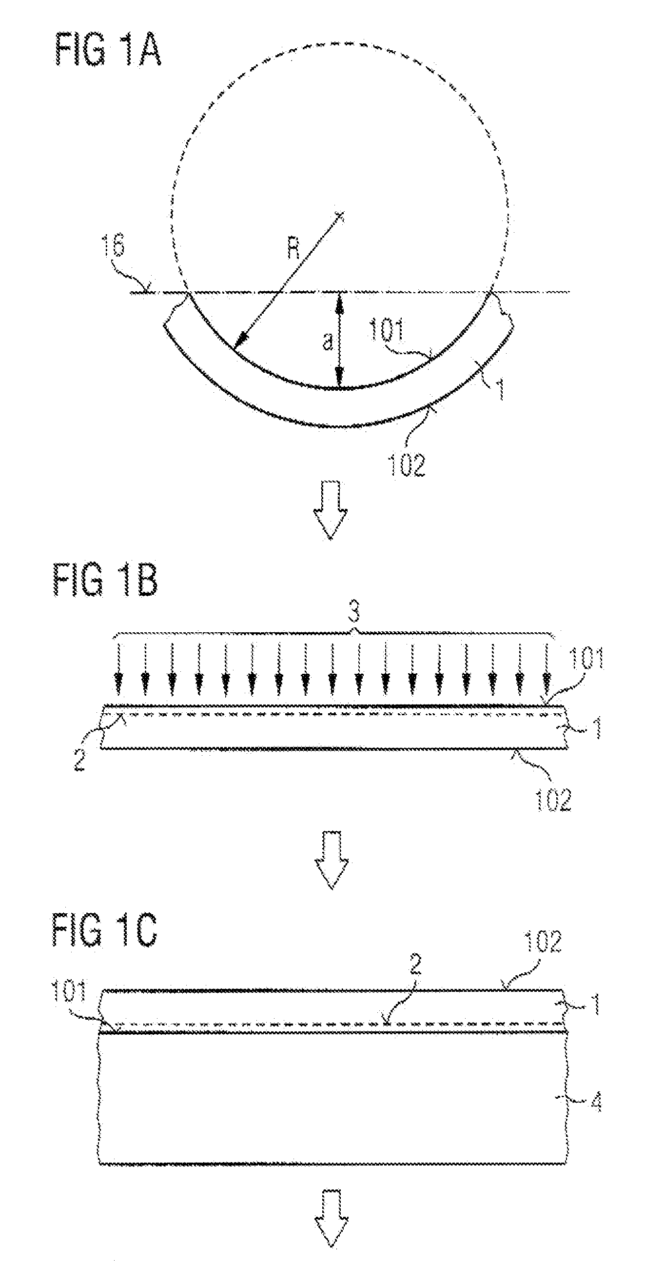
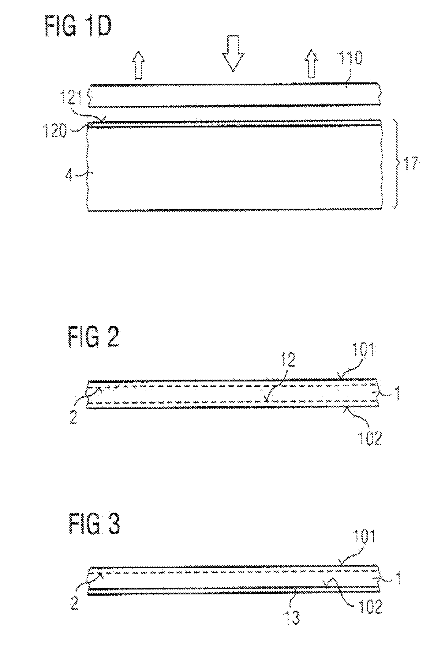
[0068] In the exemplary embodiments and figures, like or like-acting elements are identified in the same way and provided with the same respective reference numerals. The depicted elements and their size relationships to one another are basically not to be considered true to scale, but rather, individual elements, such as layers, for example, may be depicted as exaggeratedly large or exaggeratedly curved for the sake of better visualization and / or better understanding.

[0069] In a method according to the first exemplary embodiment of the first inventive method, depicted in FIGS. 1A to 1D, a quasi-substrate wafer with a subcarrier wafer and a growth layer is fabricated.

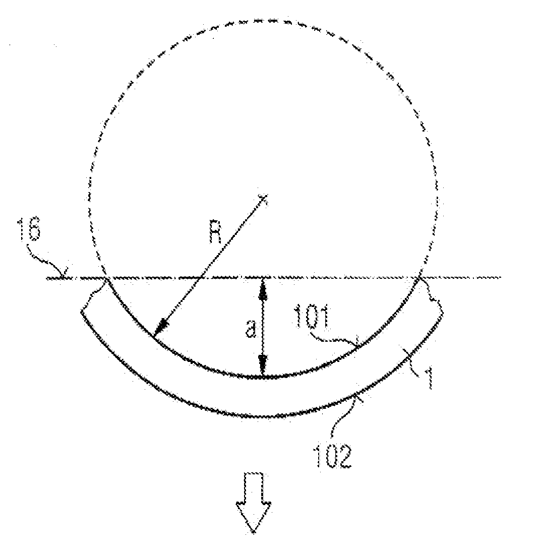
[0070] First, a growth substrate wafer1 having a first main face 101 and a second main face 102 is prepared from a nitride III compound semiconductor material, for example GaN or AlN. The growth substrate wafer 1 exhibits a stress that concavely bows first main face 101, as shown by FIG. 1A. Both first main face 101 a...


PUM

PropertyMeasurementUnit
side lengthaaaaaaaaaa
radiusaaaaaaaaaa

Abstract

Disclosed are a method of fabricating a quasi-substrate wafer (17) with a subcarrier wafer (4) and a growth layer (120), and a semiconductor body fabricated using such a quasi-substrate wafer (17). In the method of fabricating a quasi-substrate wafer (17), a growth substrate wafer (1) is fabricated that is provided with a separation zone (2) and comprises the desired material of the growth layer (120). The growth substrate wafer (1) is provided with a stress that counteracts a stress generated by the formation of the separation zone, and/or the stress generated by the formation of the separation zone is distributed, by structuring a first main face (101) of the growth substrate wafer (1) and/or the separation zone (2), to a plurality of subregions along the first main face (101). The growth substrate wafer (1) with separation zone (2) exhibits no or only slight bowing.

Description

CROSS REFERENCE TO RELATED APPLICATIONS [0001] This patent application claims foreign priority benefits under Title 35 U.S.C. to German Patent Application No. 10 2006 004 398.7, filed Jan. 31, 2006, and German Patent Application No. 10 2006 007 293.6, filed Feb. 16, 2006. The contents of these patent applications is hereby incorporated by reference in their entirety. FIELD OF THE INVENTION [0002] The invention concerns a method of fabricating a quasi-substrate wafer, and a semiconductor body fabricated using such a quasi-substrate wafer. BACKGROUND OF THE INVENTION [0003] During the performance of a method of fabricating a plurality of semiconductor bodies on a quasi-substrate wafer, a growth substrate wafer used to make the quasi-substrate wafer may become bowed. For example, WO 2005 / 004231, whose disclosure content is hereby incorporated by reference into this application, describes such a method in which a separation zone is formed in the growth substrate wafer. The formation of ...

Claims


Application Information

Patent Timeline
Patent Type & Authority Applications(United States)
IPC IPC(8): C30B23/00C30B19/00C30B25/00
CPCH01L21/76254
Inventor BRUDERL, GEORGEICHLER, CHRISTOPHSTRAUSS, UWE
Owner OSRAM OLED
Why Eureka
Try Eureka