Method for manufacturing semiconductor substrate and method for manufacturing semiconductor device

a technology of semiconductor substrate and manufacturing method, which is applied in the manufacture of final products, solid-state devices, basic electric elements, etc., can solve the problems of high difficulty in uniform treatment on a large area, glass substrate does not meet the above requirements in heat resistance, and it is difficult to provide an inexpensive large-sized semiconductor substrate (soi substrate), etc., to achieve the effect of improving the productivity of semiconductor substrates (soi substrates) and high planarity

Inactive Publication Date: 2010-05-27
SEMICON ENERGY LAB CO LTD
View PDF12 Cites 21 Cited by
  • Summary
  • Abstract
  • Description
  • Claims
  • Application Information

AI Technical Summary

Benefits of technology

[0012]In view of the above problems, another object is to increase the number of times of reprocessing a semiconductor substrate to improve the productivity.
[0026]The second single crystal semiconductor layer is separated from the first single crystal semiconductor layer utilizing compressive stress of the second single crystal semiconductor layer formed by a vapor-phase epitaxial growth method. Thus, a defect or the like does not occur in the second single crystal semiconductor layer itself, whereby heat treatment at high temperature is not needed. In addition, the second single crystal semiconductor layer after being separated has high planarity; therefore, planarization treatment such as CMP treatment is not needed. Accordingly, it becomes easy to realize a large-sized semiconductor substrate (SOI substrate).
[0027]Further, a method for separating the first single crystal semiconductor layer and the second single crystal semiconductor layer which is formed by a vapor-phase epitaxial growth method from each other is used. Thus, the first single crystal semiconductor layer is used repeatedly as a seed layer, whereby the efficiency of a reprocessing treatment is increased and the productivity of semiconductor substrates (SOI substrates) can be improved.

Problems solved by technology

In the case where a single crystal semiconductor layer is formed by such a method as disclosed in Patent Document 1, CMP treatment and / or heat treatment at high temperature is needed; therefore, it is difficult to provide an inexpensive large-sized semiconductor substrate (SOI substrate).
However, a glass substrate does not satisfy the above requirement in terms of its heat resistance.
In addition, CMP treatment is surface-polishing treatment, which has high difficulty in performing uniform treatment on a large area.
Further, in the case where a silicon wafer is reused by such a method as disclosed in Patent Document 2, the silicon wafer is polished by CMP treatment in every peeling / transferring step; therefore, the thickness of the silicon wafer is reduced gradually, so that the silicon wafer cannot be reprocessed.

Method used


Image

  • Method for manufacturing semiconductor substrate and method for manufacturing semiconductor device
  • Method for manufacturing semiconductor substrate and method for manufacturing semiconductor device
  • Method for manufacturing semiconductor substrate and method for manufacturing semiconductor device

Examples


embodiment 1

[0037]In this embodiment, an example of a method for manufacturing a semiconductor substrate (also called an SOI substrate) is described with reference to drawings.

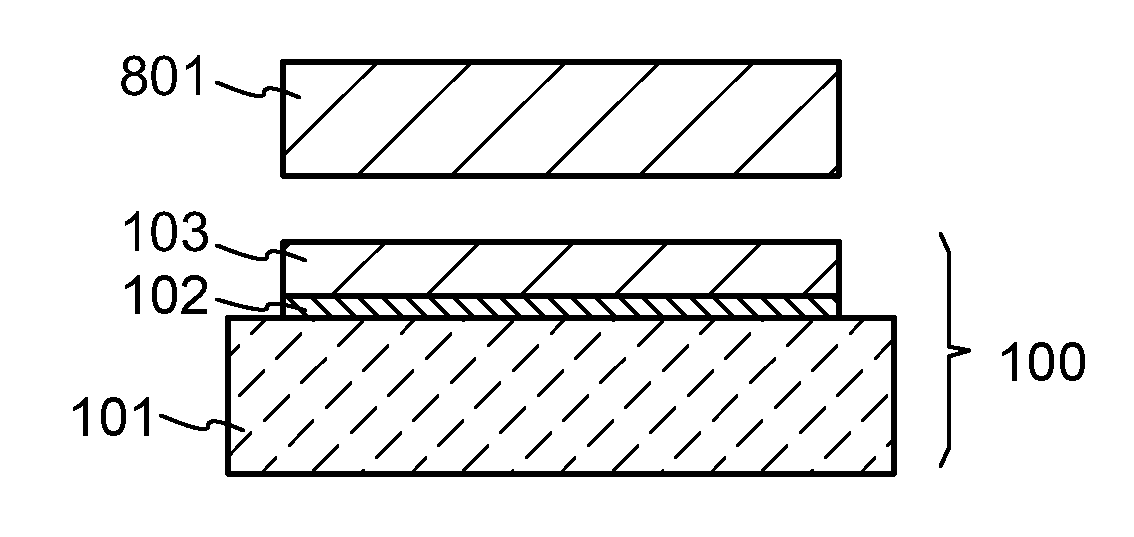
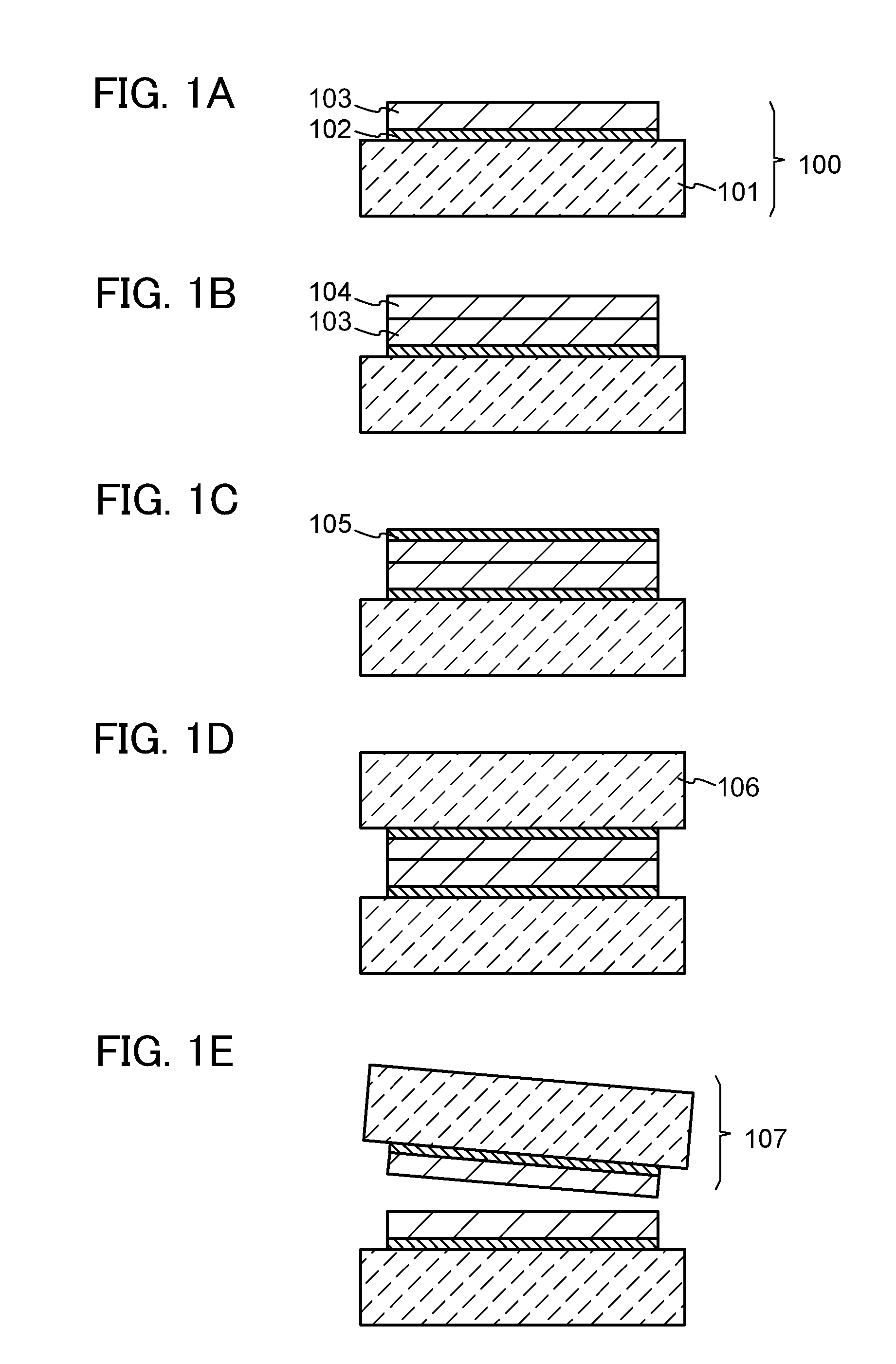
[0038]First, a first SOI substrate 100 (also called a seed substrate) is prepared (see FIG. 1A).

[0039]In the first SOI substrate 100, a first single crystal semiconductor layer 103 (also called a seed layer) can be provided over a first substrate 101 with an insulating layer 102 interposed therebetween.

[0040]An example of a method for manufacturing the first SOI substrate 100 is shown in FIG. 8. The first substrate 101 and a single crystal semiconductor substrate 801 such as a silicon wafer are prepared (see FIGS. 8A and 8B). An embrittlement layer 803 is formed in such a manner that a surface of the single crystal semiconductor substrate 801 is irradiated with an ion beam 802 which is formed of ions accelerated in the electric field, and the ions are introduced to a region of a predetermined depth (see FIG. 8C). Next the...

embodiment 2

[0072]In this embodiment, an example of a method for manufacturing a single crystal semiconductor layer is described with reference to drawings.

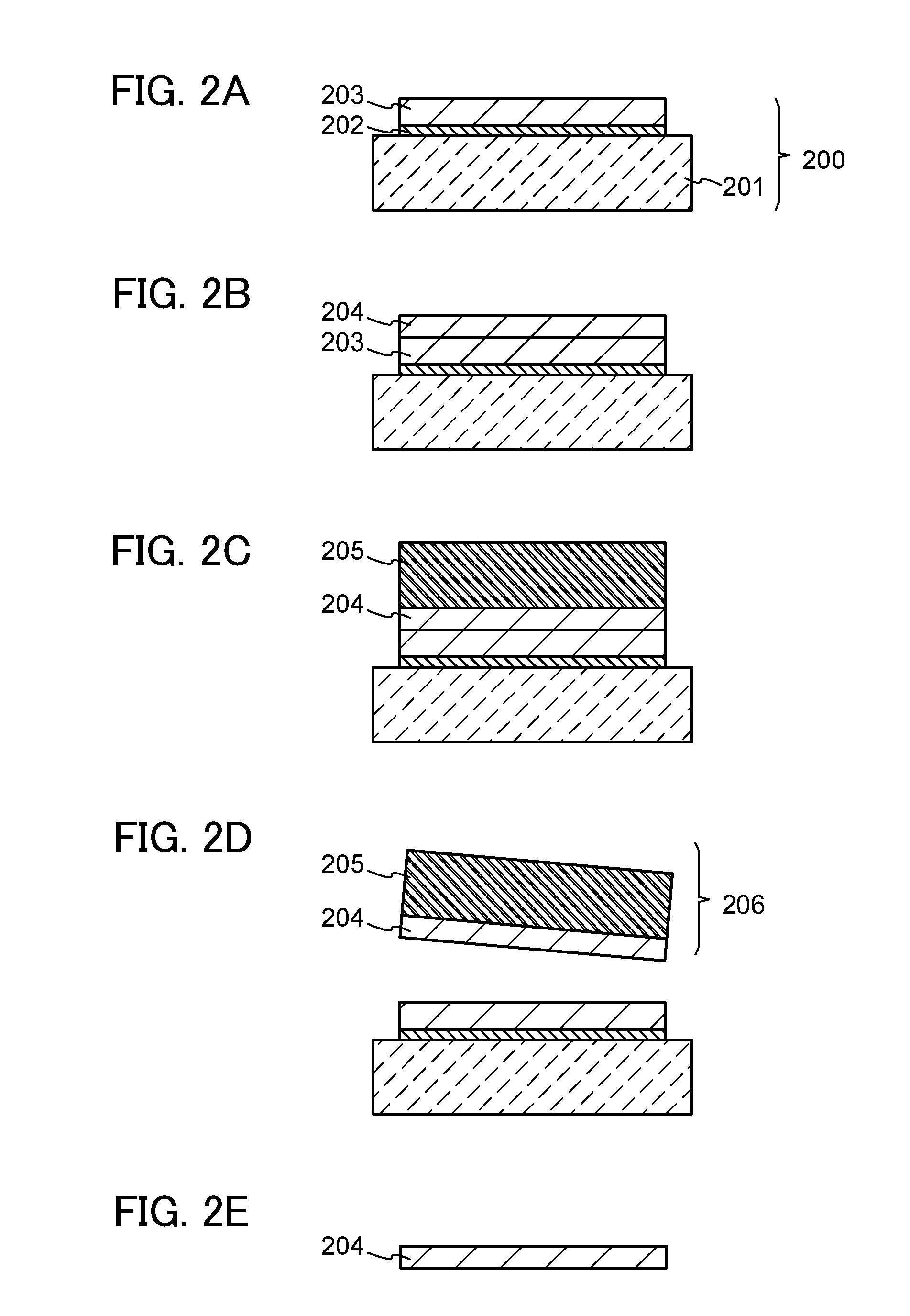
[0073]First, an SOI substrate 200 (also called a seed substrate) is prepared (see FIG.

[0074]2A).

[0075]The SOI substrate 200 may be manufactured in a manner similar to the first SOI substrate 100 described in Embodiment 1, and may have a structure where a first single crystal semiconductor layer 203 (also called a seed layer) is provided over a substrate 201 with an insulating layer 202 interposed therebetween.

[0076]That is, part of a single crystal semiconductor substrate is transferred to the substrate 201, whereby a first single crystal semiconductor layer 203 can be formed. The single crystal semiconductor substrate used here can be used repeatedly by performing the first reprocessing treatment process in a manner similar to Embodiment 1.

[0077]Next, a second single crystal semiconductor layer 204 is formed over the first single crystal se...

embodiment 3

[0091]In this embodiment, a method for manufacturing a photoelectric conversion device as an example of a method for manufacturing a semiconductor device is described with reference to drawings.

[0092]First, an SOI substrate 300 (also called a seed substrate) is prepared (see FIG. 3A).

[0093]The SOI substrate 300 may be manufactured in a manner similar to the first SOI substrate 100 described in Embodiment 1, and may have a structure where a first single crystal semiconductor layer 303 (also called a seed layer) is provided over a first substrate 301 with an insulating layer 302 interposed therebetween.

[0094]That is, part of a single crystal semiconductor substrate is transferred to the first substrate 301, whereby the first single crystal semiconductor layer 303 can be formed. The single crystal semiconductor substrate used here can be used repeatedly by performing the first reprocessing treatment process in a manner similar to Embodiment 1.

[0095]Next, a second single crystal semicon...


PUM


Abstract

An object is to manufacture a semiconductor substrate having a single crystal semiconductor layer with favorable characteristics, without requiring CMP treatment and / or heat treatment at high temperature. In addition, another object is to improve productivity of semiconductor substrates. Vapor-phase epitaxial growth is performed by using a first single crystal semiconductor layer provided over a first substrate as a seed layer, whereby a second single crystal semiconductor layer is formed over the first single crystal semiconductor layer, and separation is performed at an interface of the both layers. Thus, the second single crystal semiconductor layer is transferred to the second substrate to provide a semiconductor substrate, and the semiconductor substrate is reused by performing laser light treatment on the seed layer.

Description

BACKGROUND OF THE INVENTION[0001]1. Field of the Invention[0002]The present invention relates to a method for manufacturing a single crystal semiconductor layer. In addition, the present invention relates to a method for manufacturing a semiconductor substrate including a single crystal semiconductor film and a method for reprocessing a semiconductor substrate.[0003]2. Description of the Related Art[0004]Integrated circuits using an SOI substrate where a thin single crystal semiconductor layer is formed on an insulating surface, instead of a bulk silicon wafer, have been developed. The use of an SOI substrate can reduce parasitic capacitance between a drain of a transistor and a substrate; thus, SOI substrates are attracting attention for their ability to improve performance of semiconductor integrated circuits.[0005]A Smart Cut method is known as one of methods for manufacturing an SOI substrate (e.g., see Patent Document 1). An outline method for manufacturing an SOI substrate by ...

Claims


Application Information

Patent Timeline
Patent Type & Authority Applications(United States)
IPC IPC(8): H01L21/18H01L31/18
CPCH01L21/76254H01L31/028H01L31/075Y02E10/547H01L31/1896Y02E10/548H01L31/1804Y02P70/50H01L27/12
Inventor ISAKA, FUMITOKATO, SHOARITA, YUSHIMOMURA, AKIHISA
Owner SEMICON ENERGY LAB CO LTD
Why Eureka
Try Eureka