Dicing method and dicing device

a dicing device and dicing method technology, applied in the direction of stone-like material working tools, manufacturing tools, electric devices, etc., can solve the problems of chipping and cracking of semiconductor devices, and achieve the effect of reducing the discharge rate of cooling water, reducing the chipping of semiconductor devices, and reliable supply of cooling water

Inactive Publication Date: 2007-08-02
ABLIC INC
View PDF3 Cites 8 Cited by
  • Summary
  • Abstract
  • Description
  • Claims
  • Application Information

AI Technical Summary

Benefits of technology

[0012]In order to achieve the above-mentioned object, there is provided the following means. That is, (1) a dicing method characterized in that, in order to reliably supply a cooling water required for dicing a semiconductor wafer to a cutting portion, a dicing blade is surrounded by a case and an inside of the case is filled with the cooling water, thereby being capable of positively supplying water to the cutting portion at a time of dicing and of reducing chipping of the semiconductor device generated at the time of dicing; (2) a dicing method characterized in that a cooling water nozzle capable of continuously supplying the cooling water is attached to the case surrounding the dicing blade, and by enabling adjustment of a flow rate, a proper water pressure in the case can be ensured, thereby making it possible to sufficiently supply the cooling water to a cutting point; (3) a dicing method characterized in that a gap is formed between the case and the semiconductor wafer, and based on a gap size, a discharge rate of the cooling water to the outside of the case can be adjusted; (4) a dicing method characterized in that a brush is provided in the gap between the case and the semiconductor wafer, thereby reducing the discharge rate of the cooling water to ensure the proper water pressure in the case; (5) a dicing device, for cutting a semiconductor wafer with a dicing blade which rotates at high speed, characterized by including: the dicing blade; and a case surrounding the dicing blade and maintaining a gap between the semiconductor wafer and the case; and (6) a dicing device, for cutting a semiconductor wafer with a dicing blade which rotates at high speed, characterized by including: the dicing blade; a case surrounding the dicing blade and maintaining a gap between the semiconductor wafer and the case; and a brush provided in the gap.
[0013]According to the present invention, the cooling water can be sufficiently supplied over an entire dicing blade during cutting of the wafer, so the blade can be sufficiently cooled. Therefore, it is possible to achieve dicing which causes few numbers of chipping and cracking in the semiconductor device on the semiconductor chip. That is, a high-quality semiconductor device can be supplied in a stable manner.

Problems solved by technology

However, those developments are not sufficient, so there are still caused chipping and cracking in the semiconductor device.

Method used


Image

  • Dicing method and dicing device
  • Dicing method and dicing device
  • Dicing method and dicing device

Examples


embodiment 1

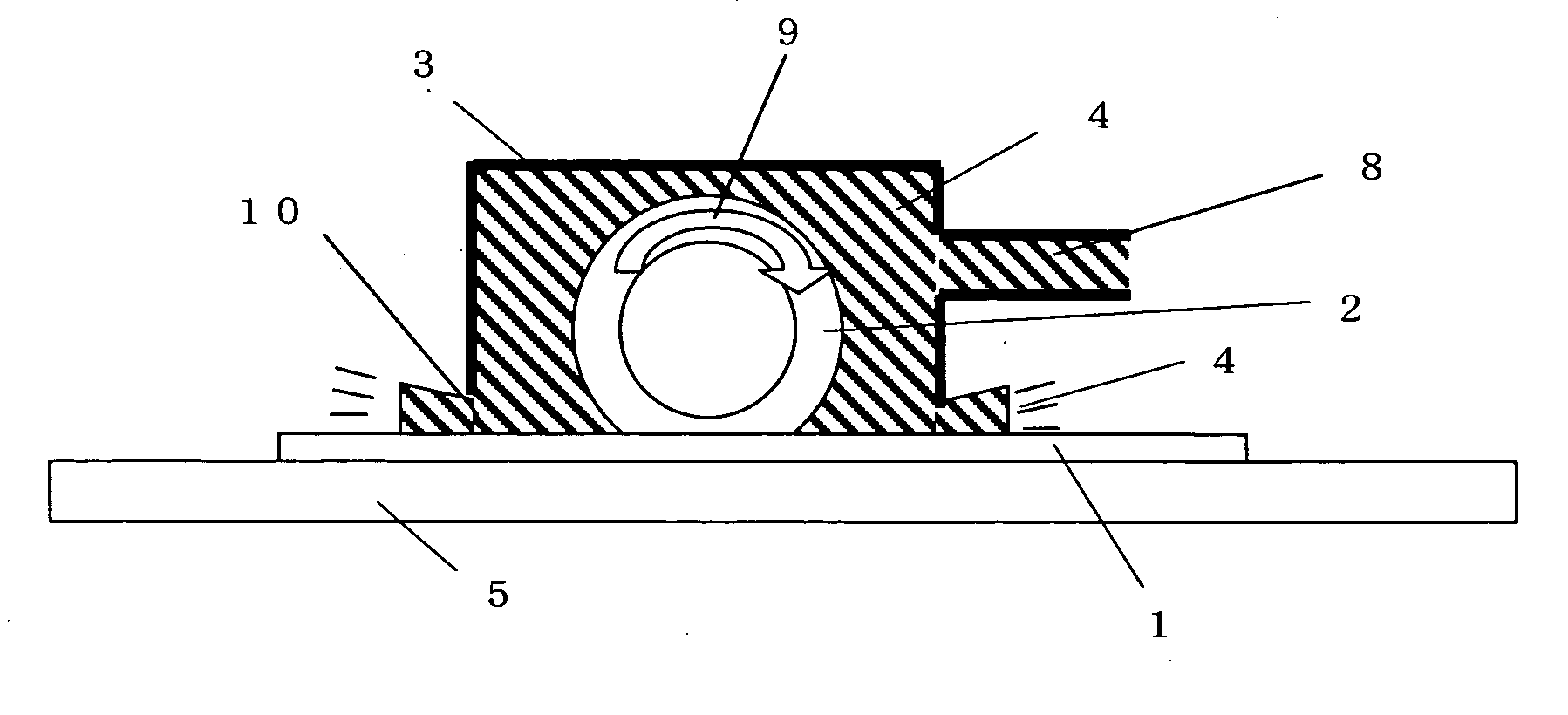
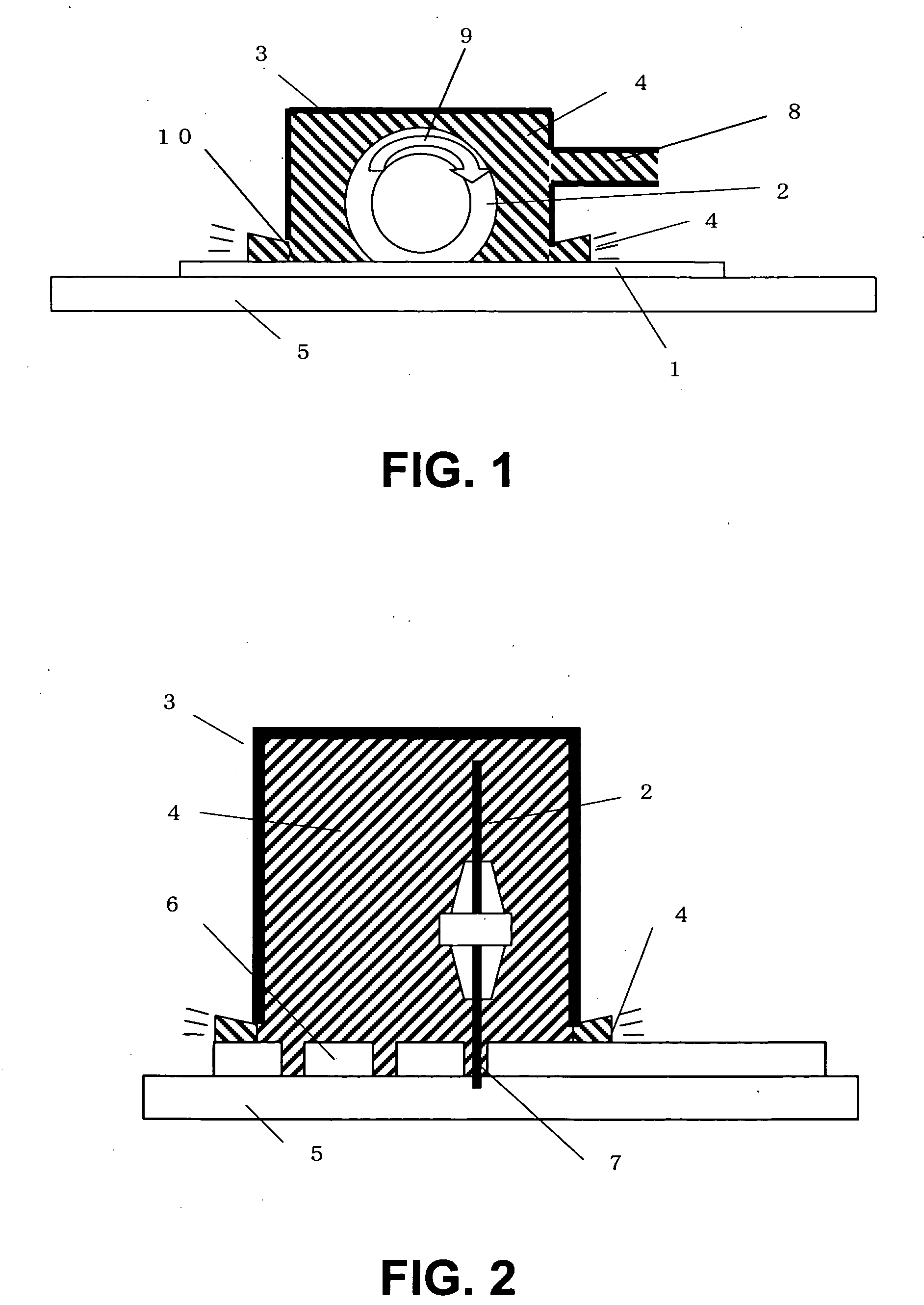
[0021]A dicing method according to a first embodiment of the present invention will be described with reference to FIGS. 1 and 2. FIG. 1 is a side view of a dicing device main portion including a dicing blade. FIG. 2 is a front view of the main portion. A semiconductor wafer 1 is bonded to a dicing tape 5 and is held on a wafer stage portion (not shown) of the dicing device. The semiconductor wafer 1 which is held is cut due to a rotation 9 of a dicing blade 2, to thereby provide individual semiconductor chips 6. The dicing blade is surrounded by a case 3 filled with a cooling water 4 and is submerged in the cooling water 4. In FIGS. 1 and 2, the case 3 surrounds the dicing blade 2 with five flat surfaces of the case 3, including an upper surface, two front surfaces, and two side surfaces. As long as only a surface facing the semiconductor wafer is opened, the case may have a spherical surface. The cooling water 4 in the case 3 is supplied from a cooling water nozzle 8 and passes th...

embodiment 2

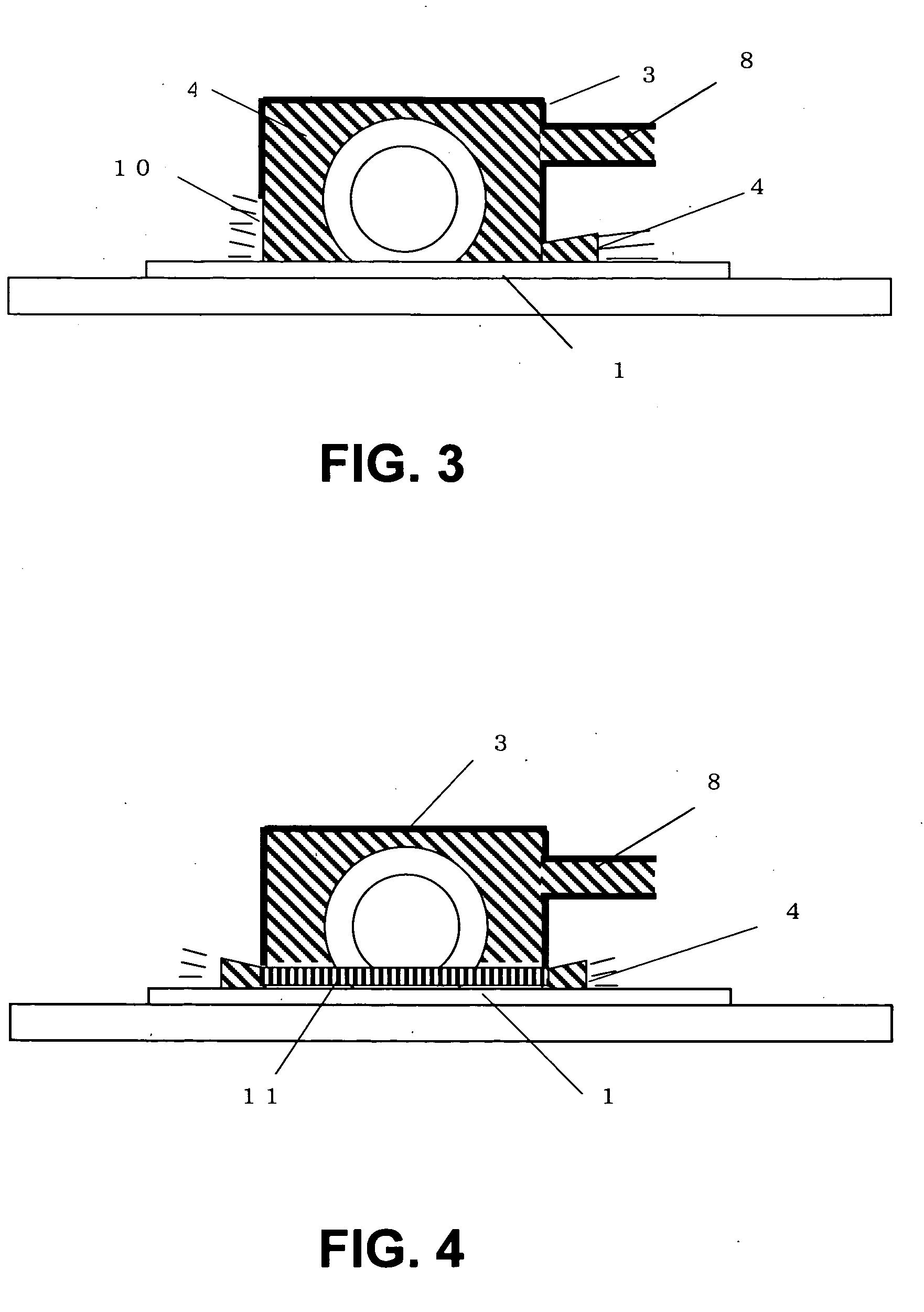
[0022]FIG. 3 shows a second embodiment of the present invention. Staying of the cutting powder around the cutting point accelerates heat generation, leading to the decrease of cutting performance, which causes chipping and cracking in the semiconductor chip. Prompt dispersion of the cutting powder generated by cutting the wafer into the cooling water to be discharged out of the case is thus desirable. In order to achieve this, a size of the gap 10 between the surface of the semiconductor wafer 1 and the case 3 is adjusted, thereby making it possible to rapidly discharge the cooling water 4 including the cutting powder to the outside of the case. A large opening in the gap 10 increases discharge rate of the cooling water and the cutting powder, enabling the cutting in the cooling water of a high degree of purity. On the other hand, a small opening in the gap 10 assures the proper water pressure in the case 3, thereby making it possible to promote the cooling of the dicing plate and t...

embodiment 3

[0023]FIG. 4 shows a third embodiment of the present invention. A brush 11 is provided in a gap between the surface of the semiconductor wafer 1 and the case 3, thereby reducing the discharge rate of the cooling water discharged from the gap and ensuring a water pressure in the case to allow the cooling water to be sufficiently supplied to the cutting point. Note that, it is preferable that a tip of the brush does not come into contact with the surface of the wafer and a slight space is maintained therebetween.


PUM

PropertyMeasurementUnit
speedaaaaaaaaaa
pressureaaaaaaaaaa
sizeaaaaaaaaaa

Abstract

A dicing blade (2) which rotates at high speed is surrounded by a case (3). A semiconductor wafer (1) is cut by a dicing device in which the case is filled with a cooling water (4). The case (3) is provided with a cooling water nozzle (8) for continuously supplying the cooling water and a gap (10) for discharging the cooling water out of the case. By adjusting a supply rate and a discharge rate of the cooling water, a proper water pressure can be applied to an inside of the case, thereby making it possible to cool the dicing blade and the cutting point with efficiency. As a result, it is possible to suppress chipping and cracking of the semiconductor device due to lack of cooling.

Description

BACKGROUND OF THE INVENTION[0001]1. Field of the Invention[0002]The present invention relates to a dicing machine and method enabling reduction of chipping and cracking both of which are caused during dicing a semiconductor wafer.[0003]2. Description of the Related Art[0004]Conventionally, a semiconductor device having a circuit formed on a semiconductor wafer is generally subjected to dicing using a dicing blade which rotates at high speed. However, in this method, heat generates when cutting the wafer by using the dicing blade, so during the dicing, the cutting is performed while supplying cooling water to a cutting portion to suppress the heat generation.[0005]In the following, an example of a conventional dicing method will be described with reference to the drawings. FIG. 5 shows a conventional dicing method, and is a side view of a main portion of a dicing device. There are provided a semiconductor wafer 1, a dicing blade 2, a cooling water 4, a dicing tape 5, and a cooling wa...

Claims


Application Information

Patent Timeline
Patent Type & Authority Applications(United States)
IPC IPC(8): B28D1/04
CPCB28D5/0076H01L21/30H01L21/78
Inventor KADOI, KIYOAKI
Owner ABLIC INC
Why Eureka
Try Eureka