Chip on board package and manufacturing method thereof

a technology of chip and packaging, applied in the direction of semiconductor devices for light sources, semiconductor/solid-state device details, lighting and heating apparatus, etc., can solve the problems of slow response, ccfl is prone to environmental pollution, and has not been put to practical use, so as to reduce manufacturing costs

Active Publication Date: 2007-08-02
SAMSUNG ELECTRONICS CO LTD
View PDF8 Cites 48 Cited by
  • Summary
  • Abstract
  • Description
  • Claims
  • Application Information

AI Technical Summary

Benefits of technology

[0018] The present invention has been made to solve the foregoing problems of the prior art and therefore an aspect of the present invention is to provide a Chip...

Problems solved by technology

Such a COB package uses an LED device as a light source and has superior capabilities to a Cold Cathode Fluorescent Lamp (CCFL), but has not been put to practical use due to its price.
The CCFL is prone to environmental pollution with use of mercury gas, slow in response, has low color reproducibility and is unsuitable for miniaturization of an LCD pa...

Method used


Image

  • Chip on board package and manufacturing method thereof
  • Chip on board package and manufacturing method thereof
  • Chip on board package and manufacturing method thereof

Examples


Embodiment Construction

[0034] Exemplary embodiments of the present invention will now be described in detail with reference to the accompanying drawings.

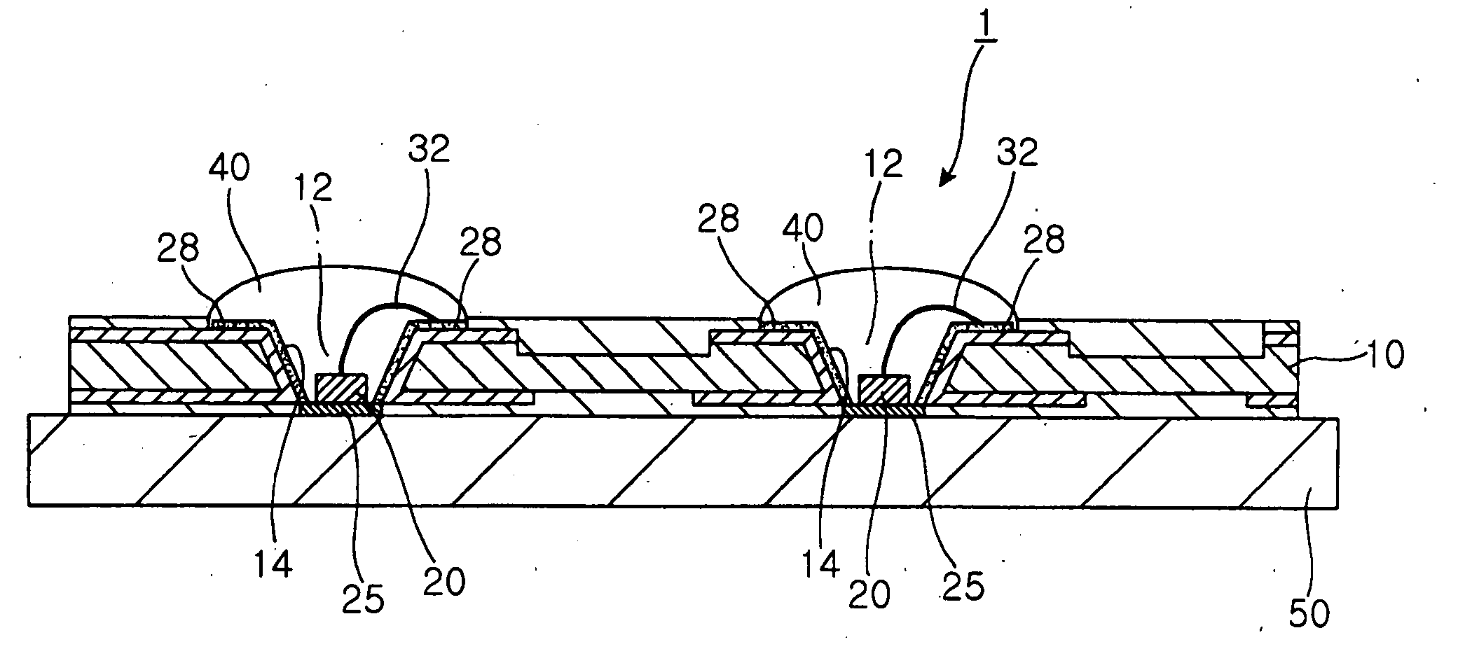
[0035] A Chip on Board (COB) package 1 according to the present invention has a substrate 10 made of a general PCB as shown in FIG. 4.

[0036] The general PCB is of a typical FR4 material with Cu layers formed on upper and lower surfaces thereof, and commercially available at a very low cost compared to the MCPCB 120.

[0037] In addition, the COB package 1 according to the present invention has through holes 12 formed in the substrate 10. Each of the through holes 12 penetrates through the substrate 10 and has a reflecting surface 14 formed therein by Ag or Au plating.

[0038] In addition, the COB package 1 according to the present invention has light sources 20 each including a submount 25 fitted to the bottom of the through hole 12, and the light sources 20 are composed of LED devices.

[0039] The submounts 25 can be made of generally used Si or AIN. An up...


PUM


Abstract

A Chip on Board (COB) package which can reduce the manufacturing costs by using a general PCB as a substrate, increase a heat radiation effect from a light source, thereby realizing a high quality light source at low costs, and a manufacturing method thereof. The COB package includes a board-like substrate with a circuit printed on a surface thereof, the substrate having a through hole. The package also includes a light source positioned in the through hole and including a submount and a dome structure made of resin, covering and fixing the light source to the substrate. The invention allows a good heat radiation effect by using the general PCB as the substrate, enabling manufacture of a high quality COB package at low costs. This in turn improves emission efficiency of the light source, ultimately realizing a high quality light source.

Description

[0001] This application claims the benefit of Korean Patent Application No. 2006-0017441 filed on Feb. 22, 2006, in the Korean Intellectual Property Office, the disclosure of which is incorporated herein by reference. BACKGROUND OF THE INVENTION [0002] 1. Field of the Invention [0003] The present invention relates to a Chip on Board (COB) package used as a light source and, more particularly, to a COB package which uses a general PCB material such as FR4 for a substrate to significantly reduce the manufacturing costs, increases a heat radiation effect from the light source to improve emission efficiency of the light source, thereby obtaining a high quality light source at low costs. [0004] 2. Description of the Related Art [0005] A Chip on Board (COB) package, that uses an LED device as a light source for a backlight unit of a TV or a monitor or a backlight for a mobile phone or a Personal Digital Assistant (PDA), is currently developed. [0006] Such a COB package uses an LED device ...

Claims


Application Information

Patent Timeline
IPC IPC(8): H01L33/00H01L21/00H01L33/58H01L33/60H01L33/62H01L33/64
CPCF21K9/00H01L33/60H05K2201/2054H01L33/62H01L2224/48091H01L2224/48227H01L2924/01078H01L2924/01079H05K1/021H05K3/244H05K2201/09827H05K2201/09981H05K2201/10106H01L2924/00014B01D21/003C02F3/28C02F2103/005E03F11/00
Inventor LEE, SEON GOOHAHM, HUN JOOKIM, DAE YEON
Owner SAMSUNG ELECTRONICS CO LTD
Why Eureka
Try Eureka