Semiconductor integrated circuit apparatus and electronic apparatus

a technology of integrated circuit and integrated circuit, which is applied in the direction of power consumption reduction, pulse technique, instruments, etc., can solve the problems of large leakage current, large chip size of integrated circuit, and large transistor siz

Inactive Publication Date: 2007-08-02
COLLABO INNOVATIONS INC
View PDF17 Cites 18 Cited by
  • Summary
  • Abstract
  • Description
  • Claims
  • Application Information

AI Technical Summary

Benefits of technology

[0016]It is therefore an object of the present invention to provide a semiconductor integrated circuit apparatus and an electronic apparatus having a power control function configured from power control MOS transistors in such a manner that leakage current and on resistance at the time of cut-off is sufficiently small in actual use.
[0017]According to an aspect of the invention, a semiconductor integrated circuit apparatus comprises a logic circuit having a plurality of NchMIS transistors and a plurality of PchMIS transistors, a first pseudo power supply line connected to a high potential side power supply terminal section of the logic circuit, a second pseudo power supply line connected to a low potential side power supply terminal section of the logic circuit, and a first NchMIS transistor having a threshold voltage smaller than an absolute value of a threshold voltage of the MIS transistors of the logic circuit, or a depletion type first NchMIS transistor. The second pseudo power supply line is connected to a drain of the first NchMIS transistor, a low potential side power supply line is connected to a source, and a voltage where a low level is a lower voltage than a potential of the low potential side power supply line and where a high level is a voltage higher than the potential of the low potential side power supply line is applied to a gate.
[0018]According to a further aspect of the invention, semiconductor integrated circuit apparatus comprises a logic circuit having a plurality of NchMIS transistors and a plurality of PchMIS transistors, a first pseudo power supply line connected to a high potential side power supply terminal section of the logic circuit, a second pseudo power supply line

Problems solved by technology

However, the low threshold voltage MOS transistor has a problem that a large leakage current occurs in a standby state.
However, with conventional semiconductor integrated circuit apparatus, there are following problems.
For example, when channel width of a MOS transistor is made large, the on resistance falls, but transistor size becomes large, and chip size of the integrated circuit also becomes large.
Further, with

Method used


Image

  • Semiconductor integrated circuit apparatus and electronic apparatus
  • Semiconductor integrated circuit apparatus and electronic apparatus
  • Semiconductor integrated circuit apparatus and electronic apparatus

Examples


embodiment 1

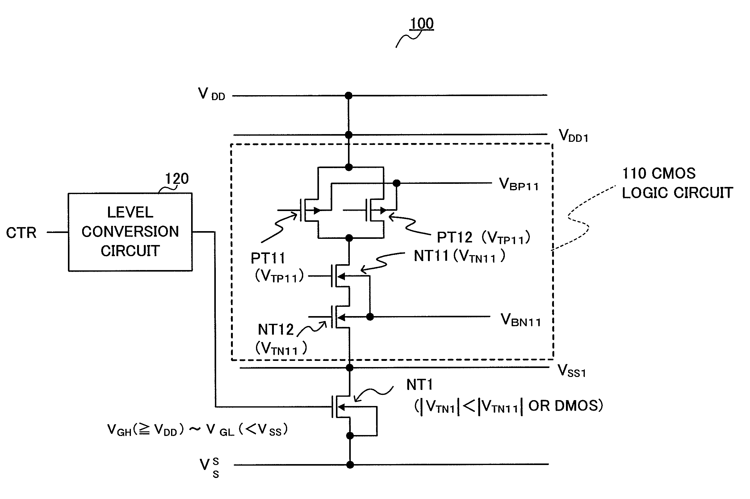
[0050]FIG. 6 is a circuit diagram showing a configuration for a semiconductor integrated circuit apparatus having a power control function according to Embodiment 1 of the present invention. This embodiment is an example applied to a semiconductor integrated circuit apparatus equipped with a CMOS logic circuit, power control NchMOS transistor, and a level conversion circuit.

[0051]In FIG. 6, semiconductor integrated circuit apparatus 100 is comprised of CMOS logic circuit 110, first pseudo power supply line VDD1 connected to a high potential side power supply terminal section of CMOS logic circuit 110, second pseudo power supply line Vss1 connected to a low potential side power supply terminal section of CMOS logic circuit 110, power control NchMOS transistor NT1 (first NchMIS transistor) connected across second pseudo power supply line VSS1 and low potential side power supply line VSS and level conversion circuit 120 for converting a signal voltage level applied to a gate of power c...

embodiment 2

[0068]Embodiment 2 is an example applied to a semiconductor integrated circuit apparatus employing a power control PchMOS transistor.

[0069]FIG. 7 is a circuit diagram showing a configuration for a semiconductor integrated circuit apparatus having a power control function according to Embodiment 2 of the present invention. This embodiment is an example applied to a semiconductor integrated circuit apparatus equipped with a CMOS logic circuit, power control PchMOS transistor, and a level conversion circuit. Portions with the same configuration as for FIG. 6 are given the same numerals and are not described.

[0070]In FIG. 7, semiconductor integrated circuit apparatus 200 is comprised of CMOS logic circuit 110, first pseudo power supply line VDD1 connected to a high potential side power supply terminal section of CMOS logic circuit 110, second pseudo power supply line VDD1 connected to a low potential side power supply terminal section of CMOS logic circuit 110, power control PchMOS tran...

embodiment 3

[0084]Embodiment 3 is an example applied to a semiconductor integrated circuit apparatus using power control NchMOS transistor NT2 electrically connected to the gate and the substrate.

[0085]FIG. 8 is a circuit diagram showing a configuration for a semiconductor integrated circuit apparatus having a power control function according to Embodiment 3 of the present invention. This embodiment is an example applied to a semiconductor integrated circuit apparatus equipped with a CMOS logic circuit, power control NchMOS transistor NT2, and a level conversion circuit. Portions with the same configuration as for FIG. 6 are given the same numerals and are not described.

[0086]In FIG. 8, semiconductor integrated circuit apparatus 300 is comprised of CMOS logic circuit 110, first pseudo power supply line VDD1 connected to a high potential side power supply terminal section of CMOS logic circuit 110, a second pseudo power supply line VSS1 connected to a low potential side power supply terminal sec...


PUM


Abstract

A semiconductor integrated circuit apparatus and an electronic apparatus having a power control function configured from power control MOS transistors in such a manner that leakage current and on resistance at the time of cut-off is sufficiently small in actual use. Semiconductor integrated circuit apparatus is comprised of a CMOS logic circuit, a second pseudo power supply line connected to a low potential side power supply terminal of the CMOS logic circuit, and a power control NchMOS transistor connected across a second pseudo power supply line and a low potential side power supply line, with the substrate and gate of power control NchMOS transistor being electrically connected. The gate and the substrate may also, for example, be connected via a current limiter utilizing, for example, a source follower of a depletion type NchMOS transistor.

Description

BACKGROUND OF THE INVENTION[0001]1. Field of the Invention[0002]The present invention relates to a semiconductor integrated circuit apparatus and an electronic apparatus having a power control function for improving current supply performance of a power control transistor at the time of operation and reducing leakage current at the time of standby.[0003]2. Description of Related Art[0004]Conventionally, methods for employing an MT-CMOS circuit (Multi Threshold-CMOS circuit) are well known as methods for implementing low power consumption of a semiconductor integrated circuit.[0005]FIG. 1 shows a circuit configuration for an MT-CMOS circuit of the related art. An MT-CMOS circuit of the related art is configured from a CMOS logic circuit, and one or both of a power control PchMOS transistor connected across a pseudo power supply line connected to a power supply terminal of the CMOS logic circuit and a high potential side power supply line (VDD), and a power control NchMOS transistor c...

Claims


Application Information

Patent Timeline
IPC IPC(8): G05F1/10
CPCH03K19/0016A47J43/24A23N12/023A47J36/10
Inventor ITO, MINORU
Owner COLLABO INNOVATIONS INC
Why Eureka
Try Eureka