Optical element, and light source unit and exposure apparatus having the same

a technology of optical elements and light sources, applied in the field of optical elements, can solve the problems of difficult fabrication of multi-layer mirrors with large curvatures, small degree of design freedom, and difficult uniform coating of evaporation, so as to achieve the effect of easy formation of multi-layer mirrors

Inactive Publication Date: 2007-08-02
CANON KK
View PDF16 Cites 10 Cited by
  • Summary
  • Abstract
  • Description
  • Claims
  • Application Information

AI Technical Summary

Benefits of technology

[0013] Accordingly, it is an exemplary object of the present invention to easily form a multilayer mirror with a large curvature, and to

Problems solved by technology

A grazing-incidence total-reflection mirror may usually maintain its reflectance higher than several scores of percentage for obliquely incident light within several degrees from the surface, but its degree of freedom in design is small.
The evaporation has a difficulty in uniformly coating as the substrate's offset from a flat surface or curvature becomes large.
Disadvantageously, a fabrication of a multilayer mirror with a large curvature is very difficult.
Debris is a critical problem for an EUV light source.
Debris disadvantageously sticks to a multilayer or collides with the multilayer, destroying its

Method used


Image

  • Optical element, and light source unit and exposure apparatus having the same
  • Optical element, and light source unit and exposure apparatus having the same
  • Optical element, and light source unit and exposure apparatus having the same

Examples


Embodiment Construction

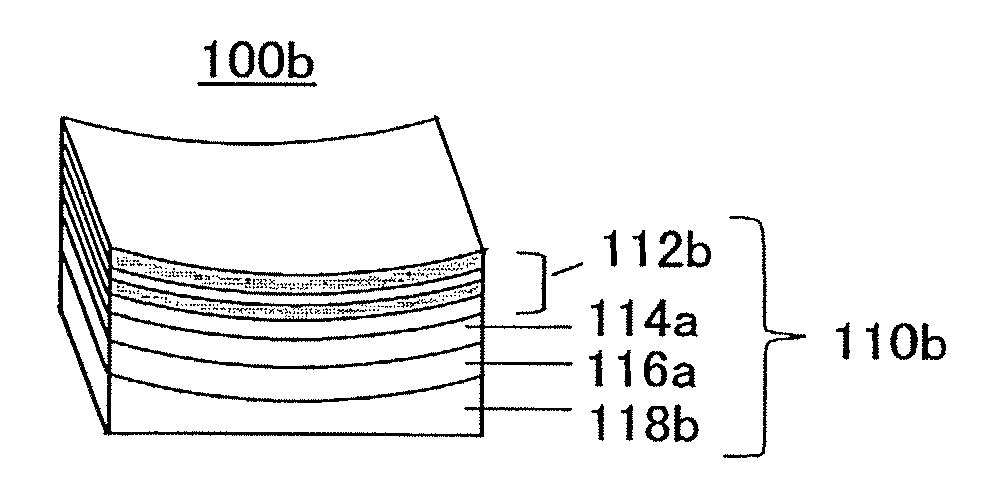
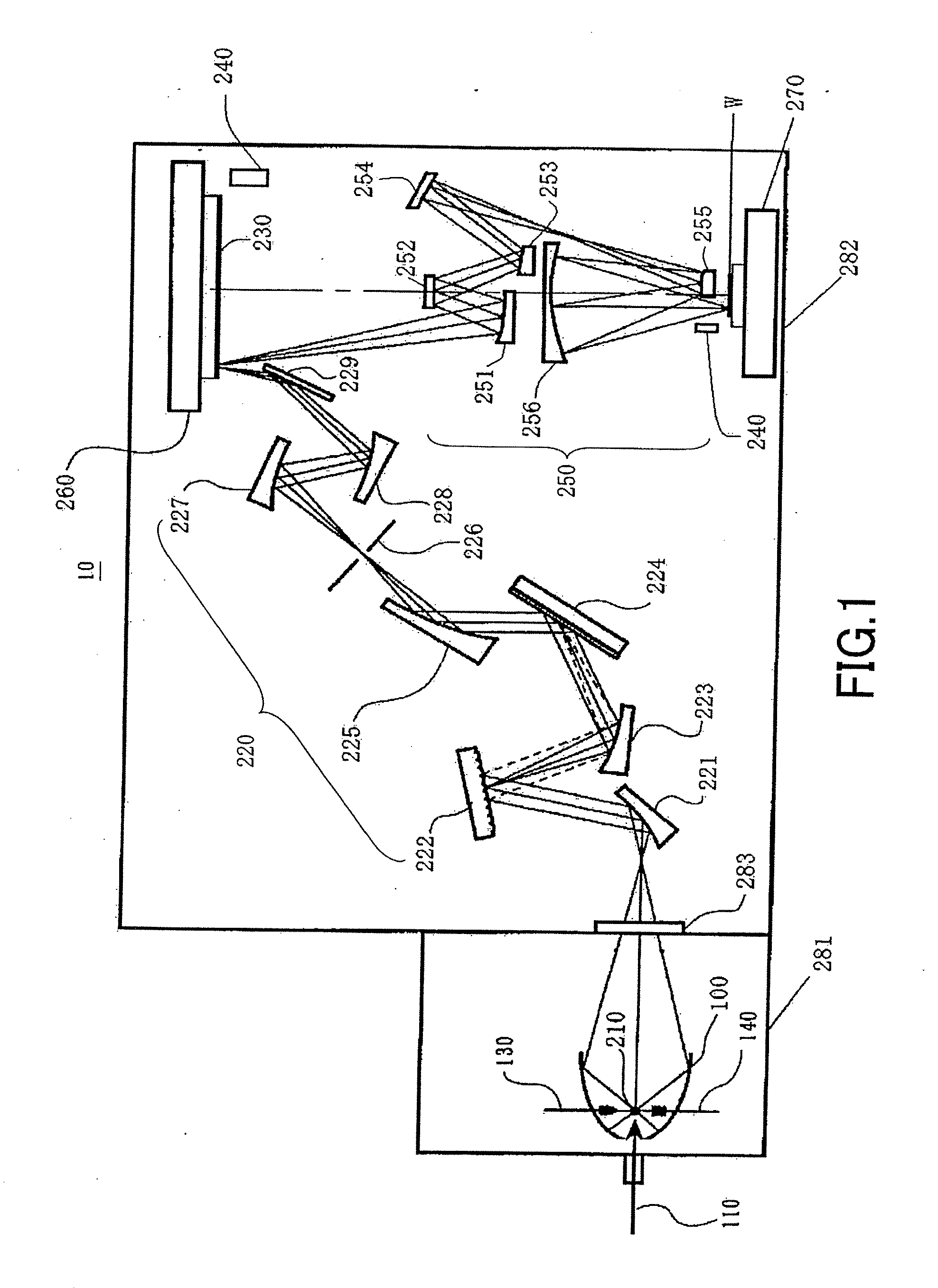
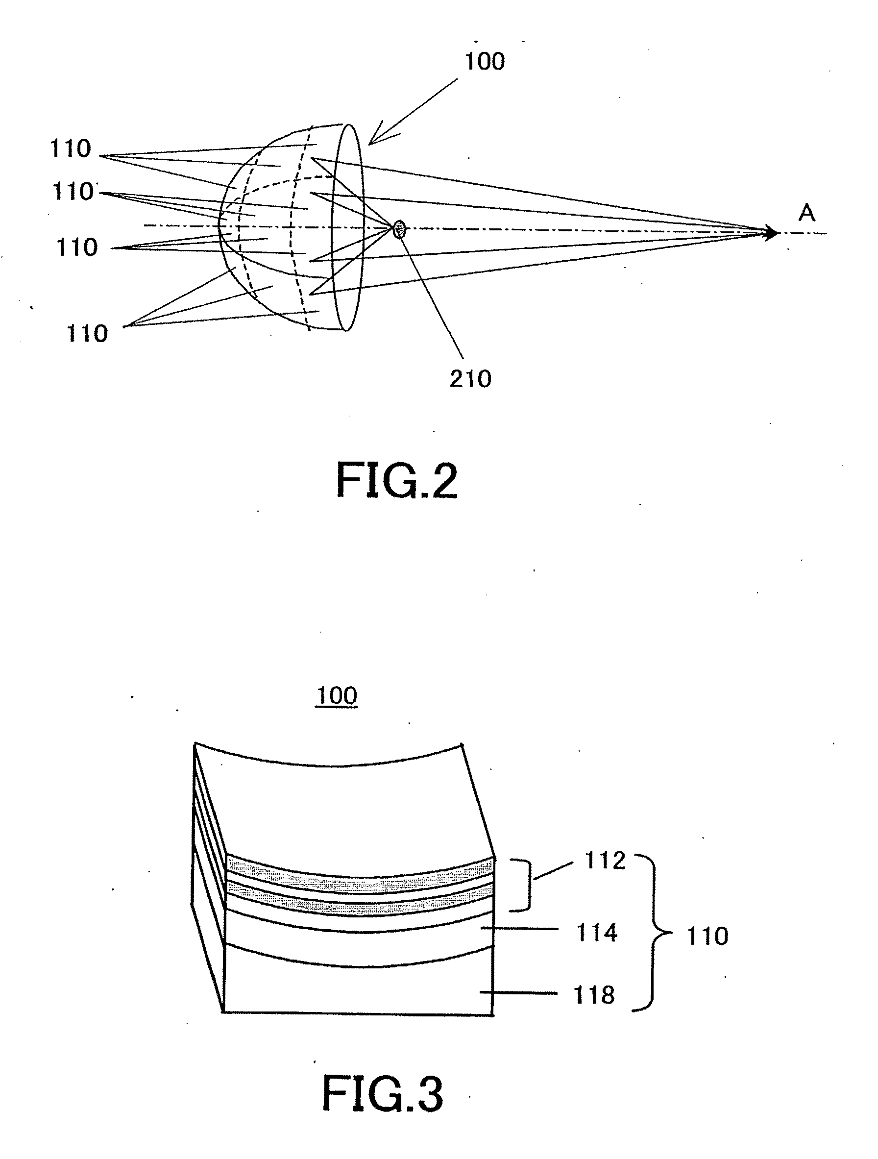
[0040] With reference to accompanying drawings, a description will now be given of an exposure apparatus 10 that uses an optical element 100 of one aspect according to the present invention. In each figure, the same reference numeral indicates a corresponding member. Here, FIG. 1 is a typical view showing the exposure apparatus 10 of one aspect of the present invention.

[0041] The inventive exposure apparatus 10 uses EUV light with a wavelength of 5 to 20 nm, for example, a wavelength of 13.4 nm as illumination light for exposure. The exposure apparatus 10 forms an arc or ring image surface, and exposes the whole area on the mask by scanning the mask and the wafer at a speed ratio of a reduction ratio. Any other method is applicable. Referring to FIG. 1, the exposure apparatus 10 includes an EUV light source 210 (221 to 229), the optical element 100, an illumination optical system 220, a catoptric reticle 230, an alignment optical system 240, a projection optical system 250, a retic...


PUM


Abstract

An optical element includes plural multilayer mirrors, wherein the multilayer mirrors are renewable.

Description

[0001] This is a divisional of prior application Ser. No. 10 / 439,711, filed May 16, 2003, now pending. The prior application is incorporated herein by reference in its entirety. [0002] This application claims the right of priority under 35 U.S.C. §119 based on Japanese Patent Application No. 2002-142454, filed on May 17, 2002, which is hereby incorporated by reference herein in its entirety as if fully set forth herein.BACKGROUND OF THE INVENTION [0003] The present invention relates generally to optical elements, and more particularly to a renewable optical element that may be reused after it deteriorates. [0004] Along with recent demands on smaller and lower profile electronic devices, fine semiconductor devices to be mounted onto these electronic devices have been increasingly demanded. For example, a design rule for a mask pattern requires an extensive formation of the image with a size of a line and space (“L & S”) of 0.1 μm or less, which will predictably shift to a formation o...

Claims


Application Information

Patent Timeline
IPC IPC(8): G02B1/10G02B5/08G02B17/06G02B27/00G03F7/20G03F7/22H01L21/027
CPCB82Y10/00G02B5/0891G02B17/0657G02B27/0043G21K2201/067G03F7/70916G03F7/70958G03F7/70975G21K1/062G03F7/70175
Inventor MASAKI, FUMITAROMIYAKE, AKIRA
Owner CANON KK
Why Eureka
Try Eureka