Dynamic Shift Register Circuit

a register circuit and shift register technology, applied in the direction of information storage, static storage, digital storage, etc., can solve the problems of serious distortion of display images, high possibility of wrong image data being received by the pixel array, and affect the display quality, so as to avoid data input errors and reduce the voltage of the cross point

Active Publication Date: 2007-08-02
AU OPTRONICS CORP
View PDF8 Cites 9 Cited by
  • Summary
  • Abstract
  • Description
  • Claims
  • Application Information

AI Technical Summary

Benefits of technology

[0009]The primary objective of this invention is to provide a dynamic shift register circuit for reducing the voltage of the cross point of two adjacent output pulses effectively and also avoiding an error of data inputting. The dynamic shift register circuit comprises a plurality of shift register units connected in series. The shift register units are controlled by a first clock signal and a second clock signal. Each of the shift register units comprises an input transistor assembly, a first output transistor, a second output transistor, a switch transistor, and a switch. The input transistor assembly has a first electrode, a second electrode, and a gate electrode. The first output transistor has a first electrode, a second electrode, and a gate electrode. The second output transistor has a first electrode, a second electrode, and a gate electrode. The switch transistor has a first electrode, a second electrode, and a gate electrode. The gate electrode of the input transistor assembly is adapted to receive the i

Problems solved by technology

Therefore, part of image data will be incorrectly displayed on pixels which are not corresponding to that the display shown is not stable and the display quality is affected.
To sum up, the signals of two adjacent output ends in the prior dynamic shift

Method used


Image

  • Dynamic Shift Register Circuit
  • Dynamic Shift Register Circuit
  • Dynamic Shift Register Circuit

Examples


Embodiment Construction

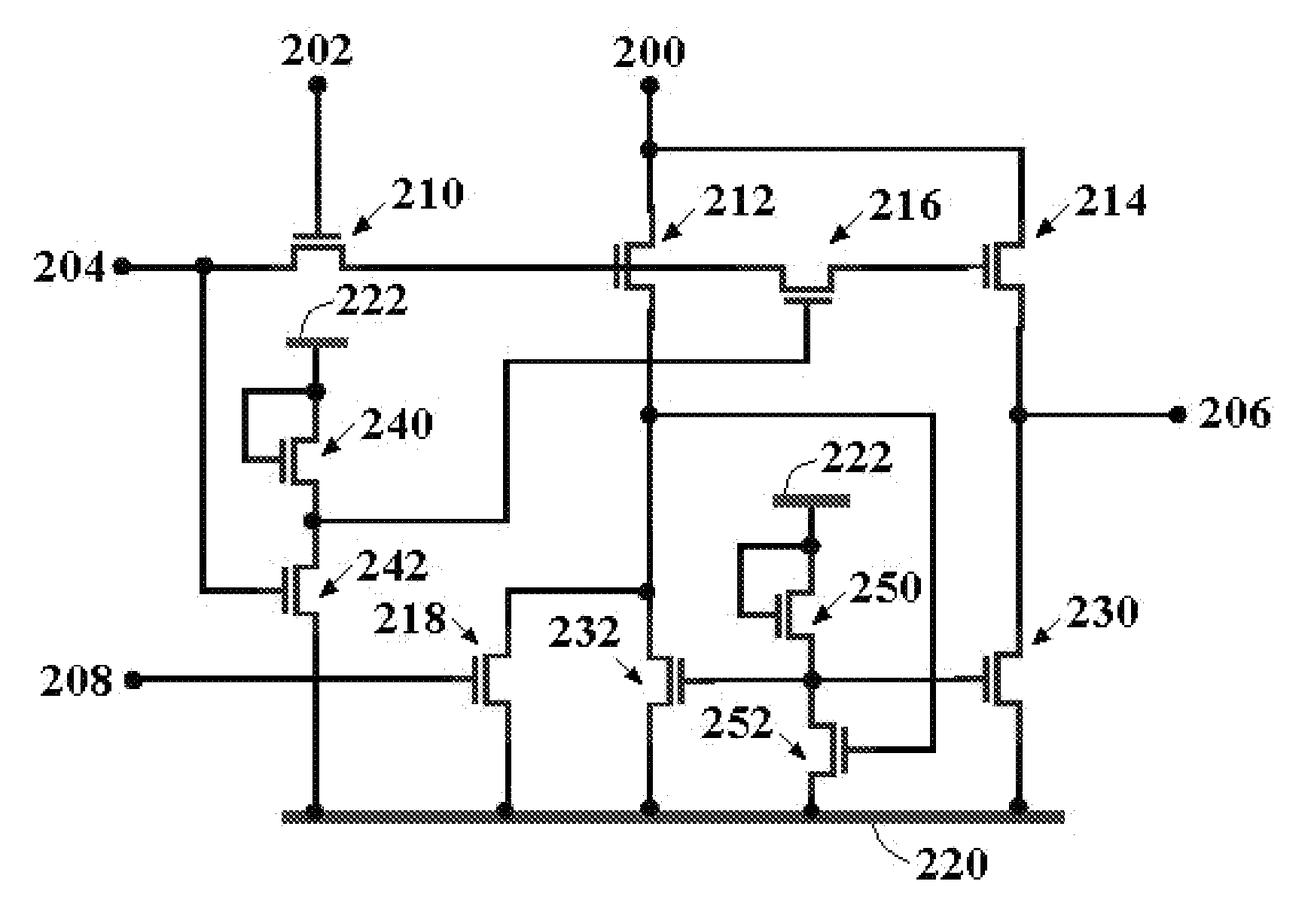
[0023]FIG. 2A shows a circuit diagram of a dynamic shift register circuit of a preferred embodiment of the present invention. The dynamic shift register circuit comprises a plurality of shift register units connected in series. The shift register units are controlled by a clock signal 200 and an inverse clock signal 202. Each of the shift register units comprises an input transistor assembly 210, a first output transistor 212, a second output transistor 214, a switch transistor 216, a switch, a fourth transistor 230, a fifth transistor 232, a sixth transistor 240, a seventh transistor 242, a eighth transistor 250, and a ninth transistor 252. The input transistor assembly 210 as shown in FIG. 2A of this embodiment is an input transistor and comprises a first electrode, a second electrode, and a gate electrode. The first output transistor 212 comprises a first electrode, a second electrode, and a gate electrode. The second output transistor 214 comprises a first electrode, a second el...


PUM


Abstract

An improved dynamic shift register circuit is disclosed. A circuit design is provided to minimize overlapping between two adjacent output pulses in the dynamic shift register circuit. In an application of analog sample-and-hold circuit, the circuit design effectively improves a distortion of sampled data caused by significant overlapping of two adjacent output pulses as control signals.

Description

[0001]This application benefits from the priority based on Taiwan Patent Application No. 095103760 filed on Jan. 27, 2006.CROSS-REFERENCES TO RELATED APPLICATIONS[0002]Not applicable.BACKGROUND OF THE INVENTION[0003]1. Field of the Invention[0004]The present invention relates to a dynamic shift register circuit, and more specifically, to a dynamic shift register circuit for minimizing overlapping between two adjacent output pulses.[0005]2. Descriptions of the Related Art[0006]Recently, Thin-Film Transistor Liquid Crystal Display (TFT-LCD) has been widely utilized in personal computer display, TV, cell phones, and digital camera. Process technique nowadays can arrange the pixel arrays and the driving circuits of the liquid crystal display on a substrate for the aim of minimizing the cost and the weights thereof. The pixel arrays comprise a plurality of scanning lines and a plurality of signal lines while the driving circuits comprise a plurality of shift register circuits, electrical...

Claims


Application Information

Patent Timeline
IPC IPC(8): G11C19/00
CPCG11C19/28
Inventor YU, JIAN-SHEN
Owner AU OPTRONICS CORP
Why Eureka
Try Eureka