Method of fabricating gate of semiconductor device using oxygen-free ashing process

Inactive Publication Date: 2007-08-02
SAMSUNG ELECTRONICS CO LTD
View PDF39 Cites 89 Cited by
  • Summary
  • Abstract
  • Description
  • Claims
  • Application Information

AI Technical Summary

Benefits of technology

[0006]According to a first embodiment of the present invention, a method of fabricating a semiconductor device includes forming a high-k dielectric film, having a dielectric constant higher than a silicon oxide film, on a semiconductor substrate including an NMOS region and a PMOS region; forming an etching target film on the high-k dielectric film; forming a photoresist pattern to expose any one region of the two regions, on the etching target film; etching the etching target film using the photoresist pattern as an etching mask; and removing the photoresist pattern using plasma formed in the presence of an oxygen-free reactive gas.
[0007]According to a second embodiment of the present invention, a method of fabricating a semiconductor device includes forming a first high-k dielectric film, having a dielectric constant higher than a silicon oxide film, on a semiconductor substrate including an NMOS region and a PMOS region; forming a second high-k dielectric film, having a dielectric constant different from that of the first high-k dielectric film

Problems solved by technology

However, the gate dielectric film may be deteriorated when passing through a plurality of process steps.
Especially, in the case where oxygen gas is used to create plasma in the ashing process, a gate dielectric film reacts with oxygen, undesirably increasing the thickness of the dielectric film and forming a charge trap site in the dielectric film.
In this way, when the gate dielectric film becomes thick and the charge trap site is created, problems such as high threshold voltage of the transistor and det

Method used


Image

  • Method of fabricating gate of semiconductor device using oxygen-free ashing process
  • Method of fabricating gate of semiconductor device using oxygen-free ashing process
  • Method of fabricating gate of semiconductor device using oxygen-free ashing process

Examples


first embodiment

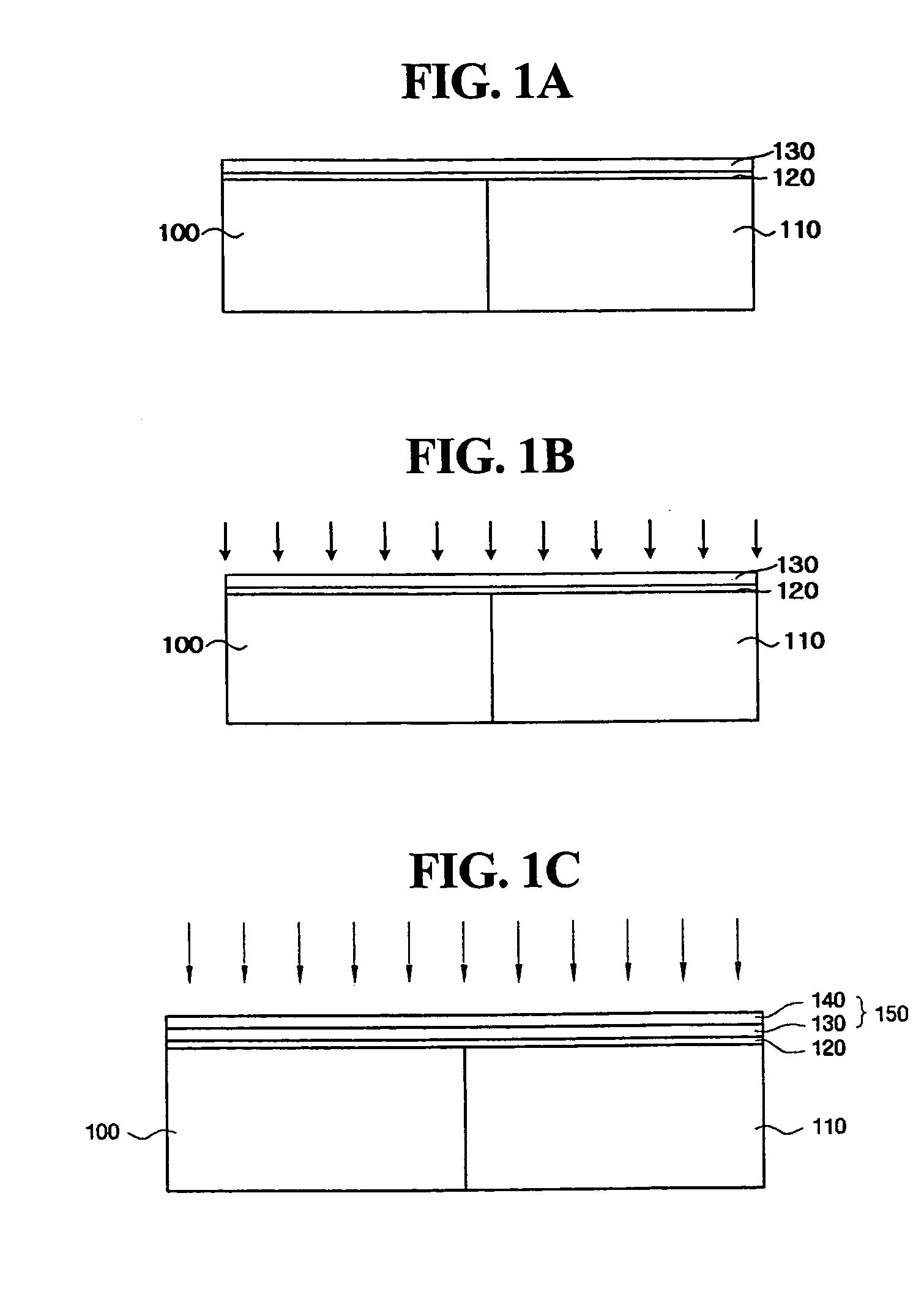
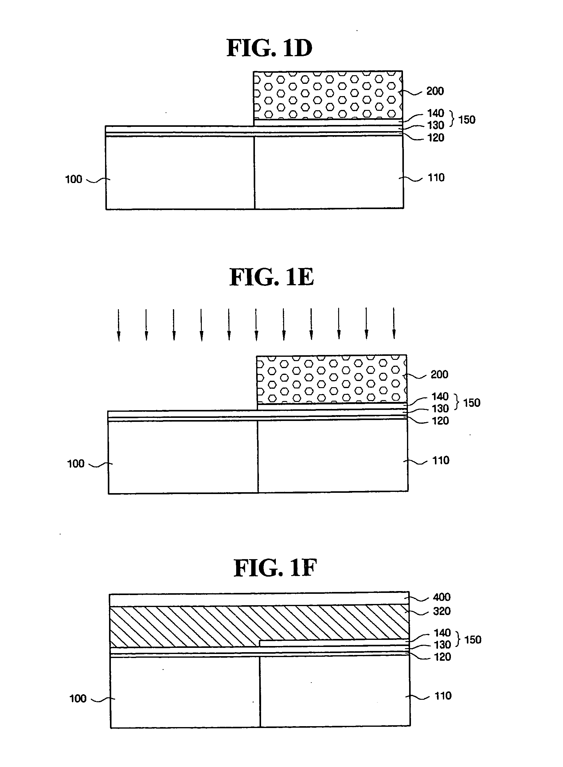
[0020]FIGS. 1A to 1G are sectional views of a semiconductor device showing the process of fabricating a semiconductor device using an oxygen-free ashing process, according to the present invention.

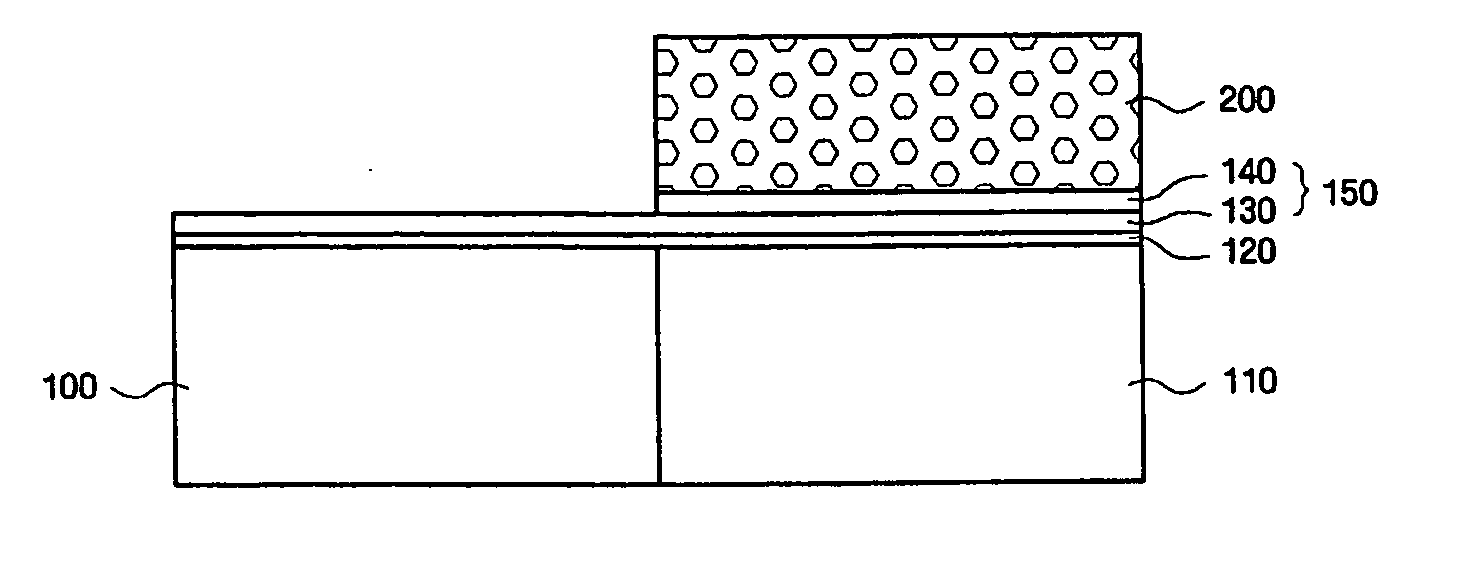
[0021]As shown in FIG. 1A, an NMOS region 100 and a PMOS region 110 are formed on a substrate, and an interfacial layer 120 is formed before forming a lower gate dielectric film 130. The interfacial layer 120, serving to prevent a reaction between the lower gate dielectric film 130 and the silicon substrate, may be formed to a thickness of 1.5 nm or less through a cleaning process using, for example, ozone (O3) gas or ozone-containing ozone water, or alternatively may be omitted. After the formation of the interfacial layer 120, the lower gate dielectric film130 is formed. In addition, a silicon oxide film (not shown) may be provided between the interfacial layer 120 and the lower gate dielectric film 130. In the case where a gate dielectric film has a stacked structure, the lower gate die...

second embodiment

[0029]FIGS. 2A to 2E are sectional views showing the process of fabricating a semiconductor device using an oxygen-free ashing process, according to the present invention.

[0030]As shown in FIG. 2A, an NMOS region 100 and a PMOS region 110 are formed, and an interfacial layer 120 and a gate dielectric film 150 are formed, as described above. In addition, a silicon oxide film (not shown) may be provided between the interfacial layer 120 and the gate dielectric film 150, and, alternatively, the interfacial layer 120 may be omitted. The gate dielectric film 150 may be provided in the form of a single-layer structure or a stacked structure, and also may be formed with a high-k dielectric film. When using the high-k dielectric film, the examples of the high-k dielectric film described above may be applied. Thereafter, although not shown in the drawing, PDA-1 may be conducted.

[0031]As shown in FIG. 2B, a conductive film 300 is formed to a thickness of 200 Å or less on the gate dielectric f...

third embodiment

[0036]FIGS. 3A to 3D are sectional views of a semiconductor device showing the process of fabricating a semiconductor device using an oxygen-free ashing process, according to the present invention.

[0037]As shown in FIG. 3A, an NMOS region 100 and a PMOS region 110 are formed, and an interfacial layer 120 and a gate dielectric film 150 are formed, through processes the same as those of the fabrication method according to the embodiments mentioned above. On the gate dielectric film 150, a multilayer conductive film 300 having a stacked structure of a first conductive film 310 and a second conductive film 315 is formed. The first conductive film 310 is 200 Å thick or less, and the second conductive film 315 is formed of material different from that of the first conductive film 310 and functions to modulate the work function of the first conductive film 310. The first conductive film 310 and the second conductive film 315 may be formed of any conductor selected from among a metal film, ...


PUM


Abstract

A method of fabricating a gate of a semiconductor device using an oxygen-free ashing process is disclosed. The method includes forming a high-k dielectric film, having a dielectric constant higher than a silicon oxide film, on a semiconductor substrate including an NMOS region and a PMOS region, forming an etching target film on the high-k dielectric film, forming a photoresist pattern to expose any one region of the two regions, on the etching target film, etching the etching target film using the photoresist pattern as an etching mask, and removing the photoresist pattern using plasma formed in the presence of an oxygen-free reactive gas.

Description

CROSS-REFERENCE TO RELATED APPLICATION[0001]This application claims priority from Korean Patent Application No. 10-2006-0009366 filed on Jan. 31, 2006 in the Korean Intellectual Property Office, the disclosure of which is incorporated herein by reference in its entirety.FIELD OF THE INVENTION[0002]The present invention relates to methods of fabricating semiconductor devices, and more particularly, to methods of fabricating semiconductor device gates.BACKGROUND OF THE INVENTION[0003]In the fabrication of semiconductors, a photolithographic process includes applying a photoresist on a semiconductor substrate to form a photoresist layer, selectively exposing the photoresist layer to light, developing the exposed photoresist layer to form a photoresist pattern, etching the region of the semiconductor substrate which is not screened by the photoresist, and removing the photoresist pattern used as the etching mask through an ashing process. As such, the ashing process is a type of etching...

Claims


Application Information

Patent Timeline
IPC IPC(8): H01L21/8238
CPCH01L21/823462H01L21/82345H01L21/823842H01L21/823857H01L21/8228
Inventor JUNG, HYUNG-SUKLEE, CHEOL-KYULEE, JONG-HOHAN, SUNG-KEEKIM, YUN-SEOK
Owner SAMSUNG ELECTRONICS CO LTD
Why Eureka
Try Eureka