

Semiconductor device
a technology of semiconductors and devices, applied in the field of semiconductor devices, can solve the problems of increasing on-resistance, failing to sufficiently effect a good inherent feature of the device, and difficult to protect the gate insulating film, etc., and achieves low on-resistance and high voltage capability.
- Summary
- Abstract
- Description
- Claims
- Application Information
AI Technical Summary
Benefits of technology
Problems solved by technology
Method used
Image

Examples
first embodiment
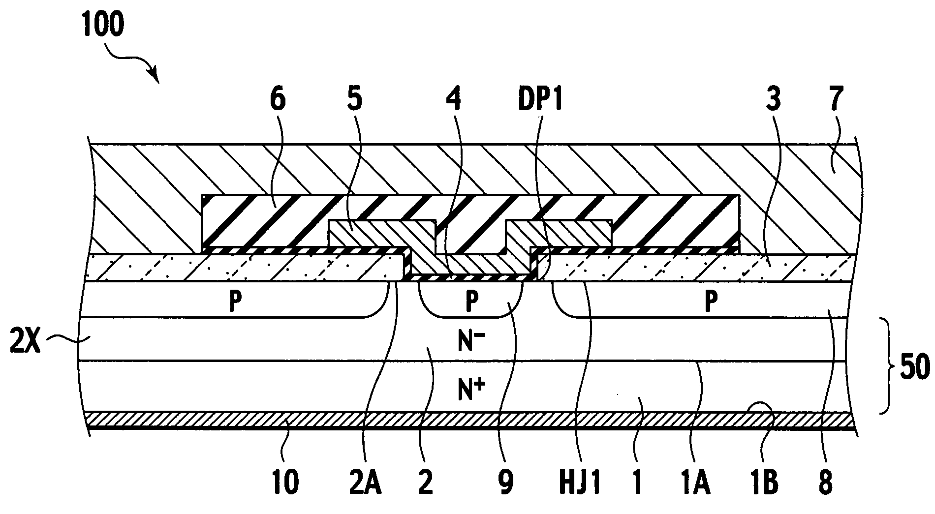
[0025]Referring to FIG. 1 to FIG. 6, a semiconductor device 100 is to be set forth, according to the first embodiment of the present invention.
[0026]FIG. 1 shows a cross sectional structure of a field effect transistor device which is the semiconductor device 100 under the present invention. In the above cross section, two unit cells are oppositely arranged. Actually however, a plurality of the unit cells are connected in parallel, thus forming the field effect transistor. The description is to be made, however, based on the above typical cross sectional structure.
[0027]At first, in terms of structure, there is provided an N+ type SiC substrate region 1, with the superscript “+” denoting a high concentration. The N+ type SiC substrate region 1 has a first face 1A on which an N− type SiC drain region 2 is formed, with the superscript “−” denoting a low concentration. The drain region 2 includes an epitaxial layer 2X grown on the SiC substrate region 1. A semiconductor substrate 50 ha...
second embodiment
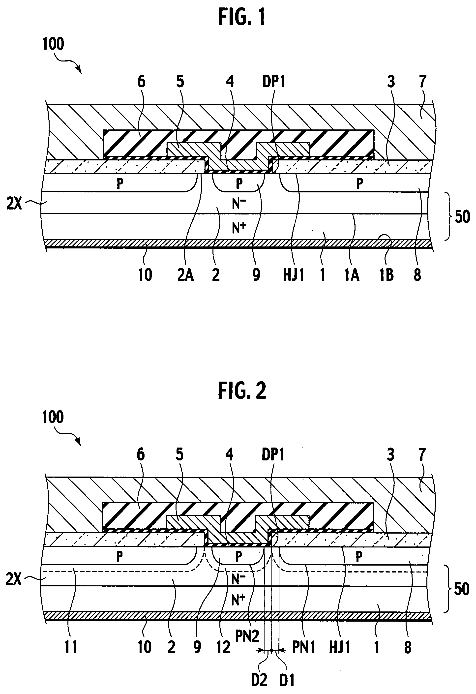
[0046]Referring to FIG. 7, the semiconductor device 100 is to be set forth, according to the second embodiment of the present invention.
[0047]The semiconductor device 100 has such a structure that a slit part 33 is formed in the N− type SiC drain region 2 below the hetero semiconductor region 3, with a P+ type hetero semiconductor 18 embedded in the slit part 33. By way of a connection part 19 made of P+ type hetero semiconductor, the P+ type hetero semiconductor 18 connects to the source electrode 7.
[0048]With the above structure, the barrier height of a hetero junction HJ2 (hetero interface) formed between the P+ type hetero semiconductor 18 and the N− type SiC drain region 2 is larger than in the case of the N type hetero semiconductor, thereby bringing about a junction featuring lower leak and higher voltage capability. A depletion layer (not shown in FIG. 7) from the above hetero junction HJ2 (hetero interface) expands, thereby bringing about an effect of suppressing an opposit...
third embodiment
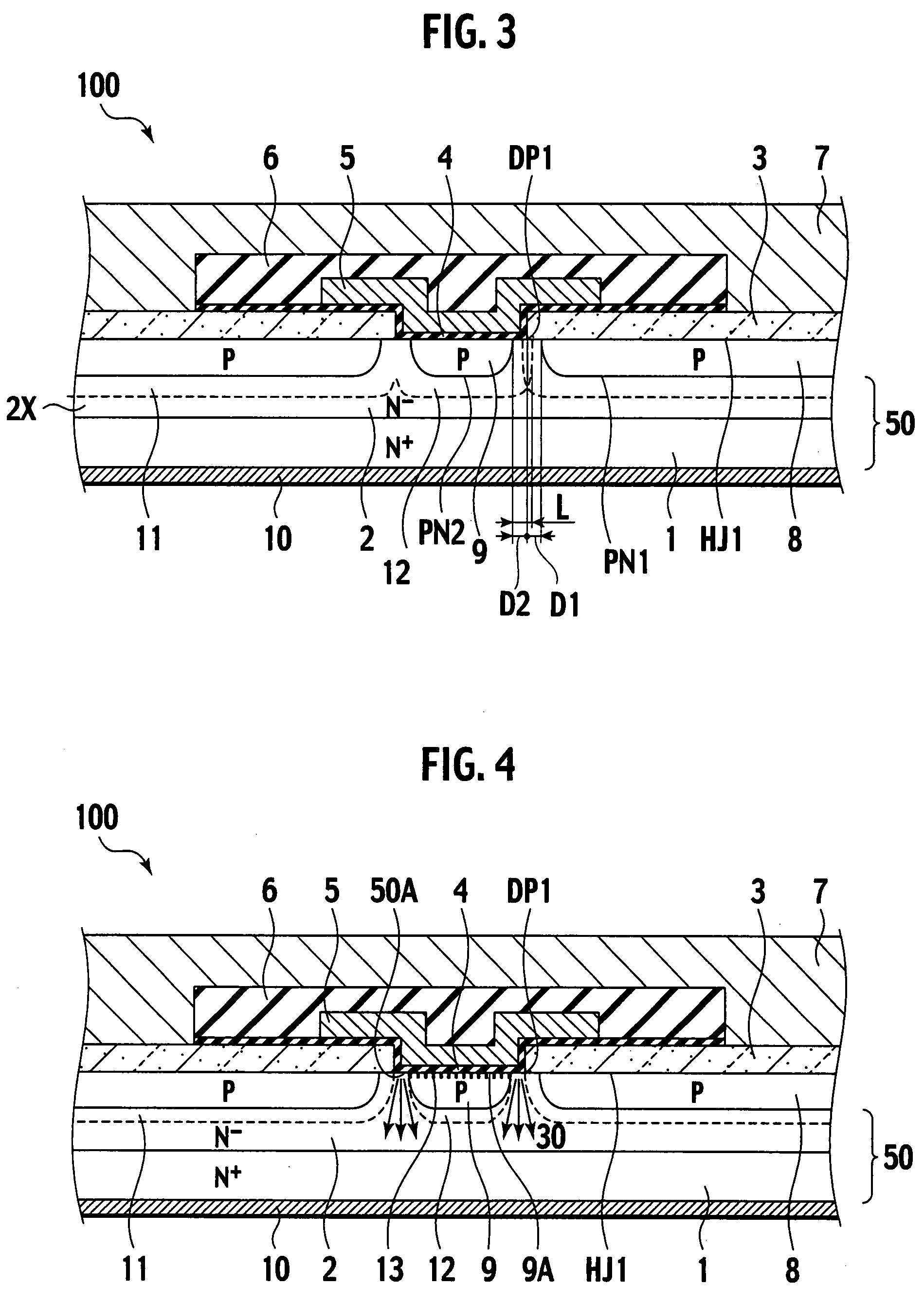
[0052]Referring to FIG. 8, the semiconductor device 100 is to be set forth, according to the third embodiment of the present invention.
[0053]The semiconductor device 100 has such a structure that a slit part 66 is formed in the N− type SiC drain region 2 below the hetero semiconductor region 3, with a Schottky electrode 20 embedded in the slit part 66.
[0054]With the above structure, a depletion layer (not shown in FIG. 8) from the Schottky electrode 20 (Schottky interface) expands, thereby bringing about an effect of suppressing the opposite leak current, together with the effect brought about by the depletion layer (not shown in FIG. 8) from the field relaxing region 9 below the gate electrode 5.
[0055]The property of the element when the element is on according to the third embodiment is equivalent to that according to the first embodiment.
[0056]Set forth below is a production method according to the third embodiment.
[0057]Specifically, a dry etching and the like is used for formin...
PUM
 Abstract
Description
Claims
Application Information