Semiconductor light emitting device and method for manufacturing the same

a technology of semiconductors and light emitting devices, which is applied in the direction of semiconductor devices, basic electric elements, electrical appliances, etc., can solve the problems of difficult selection of electrode materials, difficulty in achieving high light emission efficiency, and inability to meet the requirements of surface plasmon generation metal, etc., to achieve the effect of improving the external light emission efficiency

Inactive Publication Date: 2007-08-09
PANASONIC CORP
View PDF7 Cites 66 Cited by
  • Summary
  • Abstract
  • Description
  • Claims
  • Application Information

AI Technical Summary

Benefits of technology

[0028]In addition, the LED structure of Document 1 has less ability to dissipate heat. To achieve high ability to dissipate heat, the p electrode needs to be mounted on a mounting substrate made of a material having a high thermal conductivity. When mounting is performed in this manner, heat generated in the active layer 1003 can be easily transferred via the thin intermediate layer 1004 to the mounting substrate. However, in the structure of Document 1, when the p electrode is mounted, a surface of the metal 1005 is adhered via solder to the mounting substrate, so that the unevenness of the metal / air interface is eliminated. Therefore, it is not possible to achieve light emission of surface plasmons due to the unevenness of the interface.
[0045]With this method, a semiconductor light emitting device having an improved external light emission efficiency can be produced.

Problems solved by technology

However, the conventional technique described in Document 1 has difficulty in achieving a high light emission efficiency during current injection for the following reason.
Firstly, in the conventional LED of Document 1, it is difficult to select an electrode material.
Although a metal for generating surface plasmons is used as an electrode in this LED, a metal suitable for generation of surface plasmons is not always suitable as an electrode material.
However, since Al has a low work function, Al is not suitable as an electrode material and is difficult to achieve ohmic contact.
As a result, when Al is used in a semiconductor light emitting device, the voltage efficiency is low.
Also, in the conventional LED, it is difficult to improve the efficiency of energy conversion from electron-positive hole pairs into surface plasmons while keeping the performance.
However, when the intermediate layer 1004 is considerably thin, it is difficult to control overflow of electrons from the active layer 1003, resulting in a decrease in efficiency of formation of electron-positive hole pairs.
Also, when the intermediate layer 1004 having the p-type impurity is considerably thin, a variation in film thickness of the intermediate layer 1004 is likely to cause a short circuit of the active layer 1003 and the p electrode (the metal 1005), resulting in occurrence of leakage.
Also, in the structure of Document 1, since scattering due to a rough surface is utilized, it is difficult to achieve efficient light emission, resulting in a low efficiency of light emission from surface plasmons.

Method used


Image

  • Semiconductor light emitting device and method for manufacturing the same
  • Semiconductor light emitting device and method for manufacturing the same
  • Semiconductor light emitting device and method for manufacturing the same

Examples


first embodiment

[0065]—Configuration of Semiconductor Light Emitting Device—

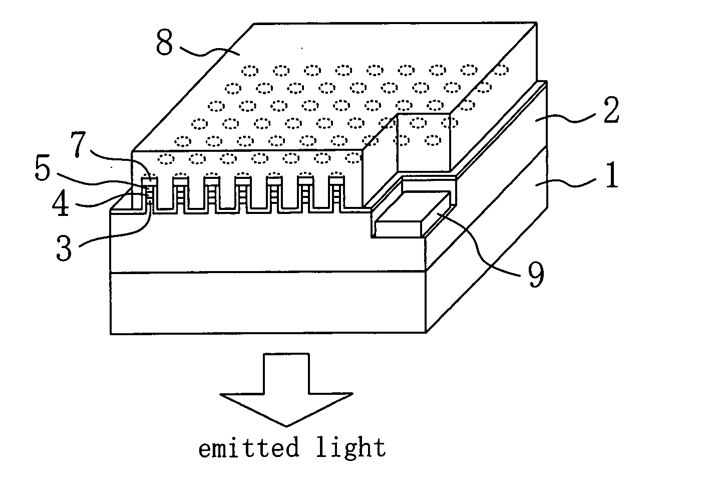
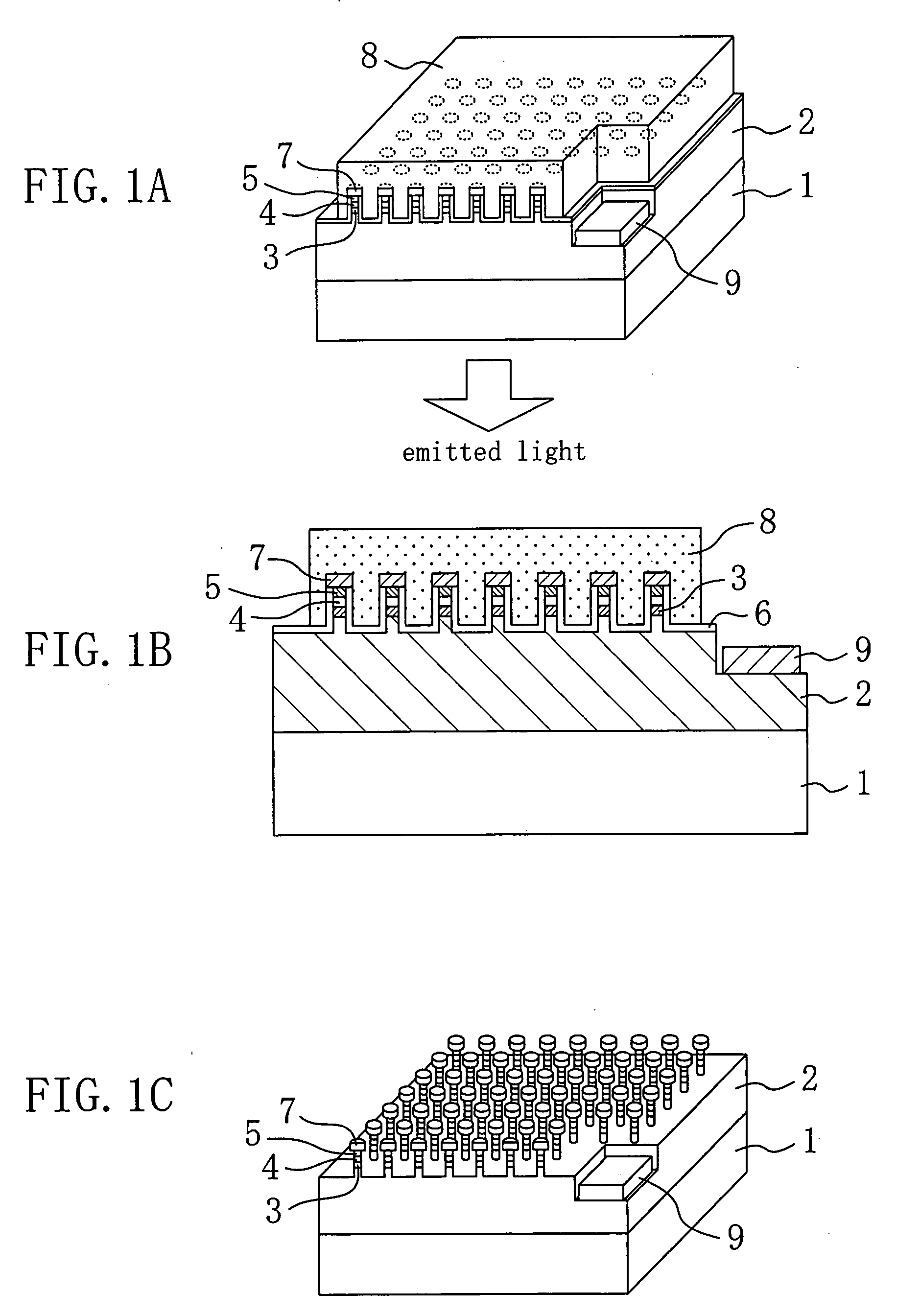
[0066]FIG. 1A is a perspective view of a semiconductor light emitting device according to a first embodiment of the present invention. FIG. 1B is a cross-sectional view of the semiconductor light emitting device of this embodiment, taken along a line passing through an n electrode 9. FIG. 1C is a perspective view of the semiconductor light emitting device, where a plasmon generating layer 8 and an insulating layer 6 are not illustrated. A cross-section passing through the n electrode 9 is also illustrated in FIG. 1A for the sake of easy understanding.

[0067]As illustrated in FIGS. 1A and 1B, the semiconductor device of this embodiment comprises: a transparent substrate 1 made of sapphire or the like; a semiconductor multilayer film which is formed on the transparent substrate 1 by crystal growth and is made of a GaN compound semiconductor; a p electrode 7 formed on the semiconductor multilayer film; an insulating layer 6 whi...

second embodiment

[0127]FIG. 10A is a perspective view of a semiconductor light emitting device according to a second embodiment of the present invention. FIG. 10B is a cross-sectional view of the semiconductor light emitting device, taken along a line passing through an n electrode 9. FIG. 10C is a perspective view of the semiconductor light emitting device of this embodiment, where a plasmon generating layer 8 and an insulating layer 6 are not illustrated.

[0128]The semiconductor light emitting device of this embodiment is different from the semiconductor light emitting device of the first embodiment in that holes penetrating through at least an active layer 3 of a semiconductor multilayer film are formed and arranged in a two-dimensional periodic manner. For example, the holes each have a diameter of 150 nm, and are arranged in a square lattice having an interval of 325 nm.

[0129]The semiconductor light emitting device of this embodiment is also different from the semiconductor light emitting device...

third embodiment

[0136]FIG. 12 is a cross-sectional view of a semiconductor light emitting device according to a third embodiment of the present invention.

[0137]In the semiconductor light emitting devices of the first and second embodiments, the continuous plasmon generating layer 8 is formed to fill the minute unevenness formed in the semiconductor multilayer film. In contrast to this, as illustrated in FIG. 12, in the semiconductor light emitting device of this embodiment, holes having a diameter of about 150 nm which penetrate through an active layer 3 are formed in a semiconductor multilayer film, and a plurality of microspheres 12 made of Al, Ag, Au or the like are buried inside the hole. In the semiconductor light emitting device of this embodiment, the peak wavelength of emitted light is in an ultraviolet region of 380 nm, and therefore, Al is preferably used as a material for the microsphere 12.

[0138]Also, a metal layer 18 which is provided on an insulating layer 6 and a p electrode 7 fills ...


PUM


Abstract

A semiconductor light emitting device comprises a semiconductor multilayer film including an active layer for generating light, a p electrode formed on the semiconductor multilayer film, and a plasmon generating layer, which are provided on a substrate. A portion of the semiconductor multilayer film including at least the active layer forms a plurality of rods. The plasmon generating layer (8) fills between each rod. The plasmon generating layer (8) is formed of a material having a negative dielectric constant at the wavelength of emitted light. The rods are arranged in a periodic manner.

Description

BACKGROUND OF THE INVENTION[0001]1. Field of the Invention[0002]The present invention relates to a light emitting device employing a semiconductor and a method for manufacturing the light emitting device.[0003]2. Description of the Related Art[0004]Of semiconductor light emitting devices, Light Emitting Diodes (LEDs) are easier to manufacture and control than semiconductor lasers, and are expected as low-cost light sources for illumination and communication. However, LEDs have problems, such as a low external quantum efficiency, a poor directivity of emitted light, and the like. As used herein, the “external quantum efficiency” refers to an efficiency with which implanted carriers produce light obtained outside an LED.[0005]There are two factors responsible for the low external quantum efficiency. One factor is a low internal quantum efficiency (efficiency with which implanted carriers can be converted into photons), and the other factor is a low light extraction efficiency (efficie...

Claims


Application Information

Patent Timeline
Patent Type & Authority Applications(United States)
IPC IPC(8): H01L33/00H01L31/12H01L27/15H01L29/26H01L33/48H01L33/06H01L33/32H01L33/40
CPCH01L33/08H01L33/20H01L33/32H01L2933/0083H01L33/44H01L33/46H01L33/40H01L2224/14
Inventor ORITA, KENJI
Owner PANASONIC CORP
Why Eureka
Try Eureka