Semiconductor device manufacturing method and semiconductor device manufacturing apparatus

a semiconductor device and manufacturing method technology, applied in semiconductor devices, solid-state devices, coatings, etc., can solve the problems of epoxy resin being easily discolored by high temperature exposure, method and potting method, and needing to reduce the variation in weight of mini tablets, etc., to achieve stable shape

Inactive Publication Date: 2007-08-09
SHARP KK
View PDF12 Cites 13 Cited by
  • Summary
  • Abstract
  • Description
  • Claims
  • Application Information

AI Technical Summary

Benefits of technology

[0020]An object of the present invention is to provide a semiconductor device manufacturing method with high accuracy, reduction in loss of material and less generation of voids in a way of sealing with liquid-state resin (particularly, silicone resin).

Problems solved by technology

Therefore, they have more faults in comparison with the normal tablet in the case of FIG. 16A, which causes a need to decrease variation in weight of the mini tablet.
However, the epoxy resin has a disadvantage of being easily discolored by exposure to high temperature.
However, the above-described conventional semiconductor device manufacturing methods, specifically, the casting method and the potting method have the disadvantages of the low dimensional accuracy of a package, a high manufacturing cost as a consequence of much time and / or labor necessary for the manufacturing, and the frequent occurrence of voids as a consequence of the entry of air into a package.
However, the transfer molding method has a disadvantage of increase in material cost due to superfluous resin generated in the runner portion and so on.
Particularly, in the case where silicone resin is used as a sealing resin in order to manufacture a semiconductor device for the car-onboard use, the silicone resin is more expensive than the epoxy resin in unit price.

Method used


Image

  • Semiconductor device manufacturing method and semiconductor device manufacturing apparatus
  • Semiconductor device manufacturing method and semiconductor device manufacturing apparatus
  • Semiconductor device manufacturing method and semiconductor device manufacturing apparatus

Examples


first embodiment

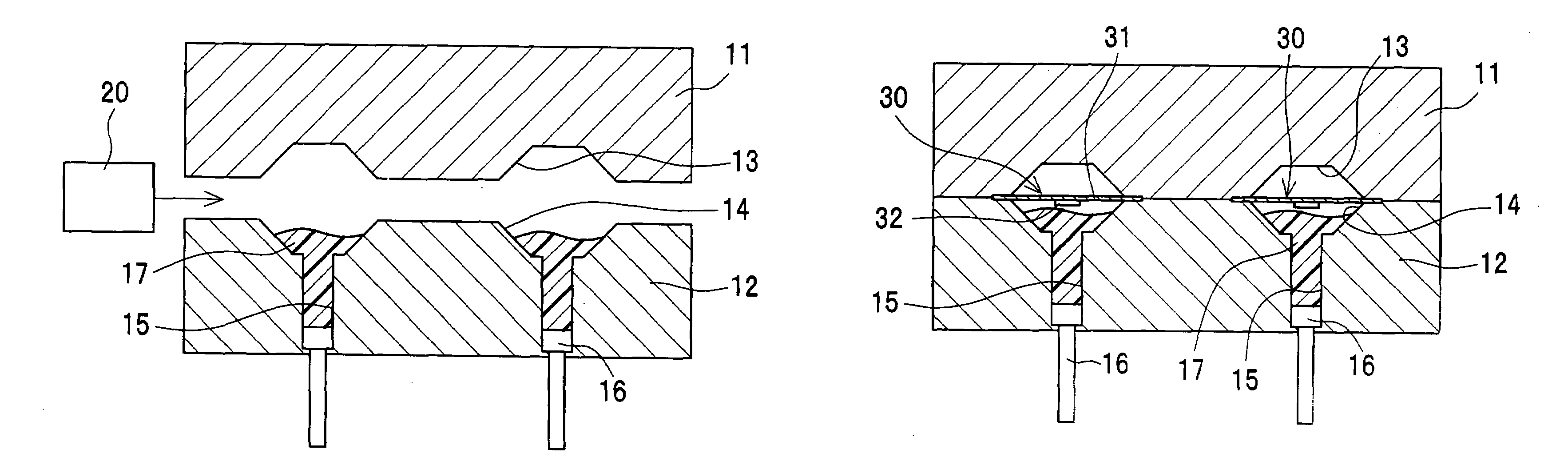
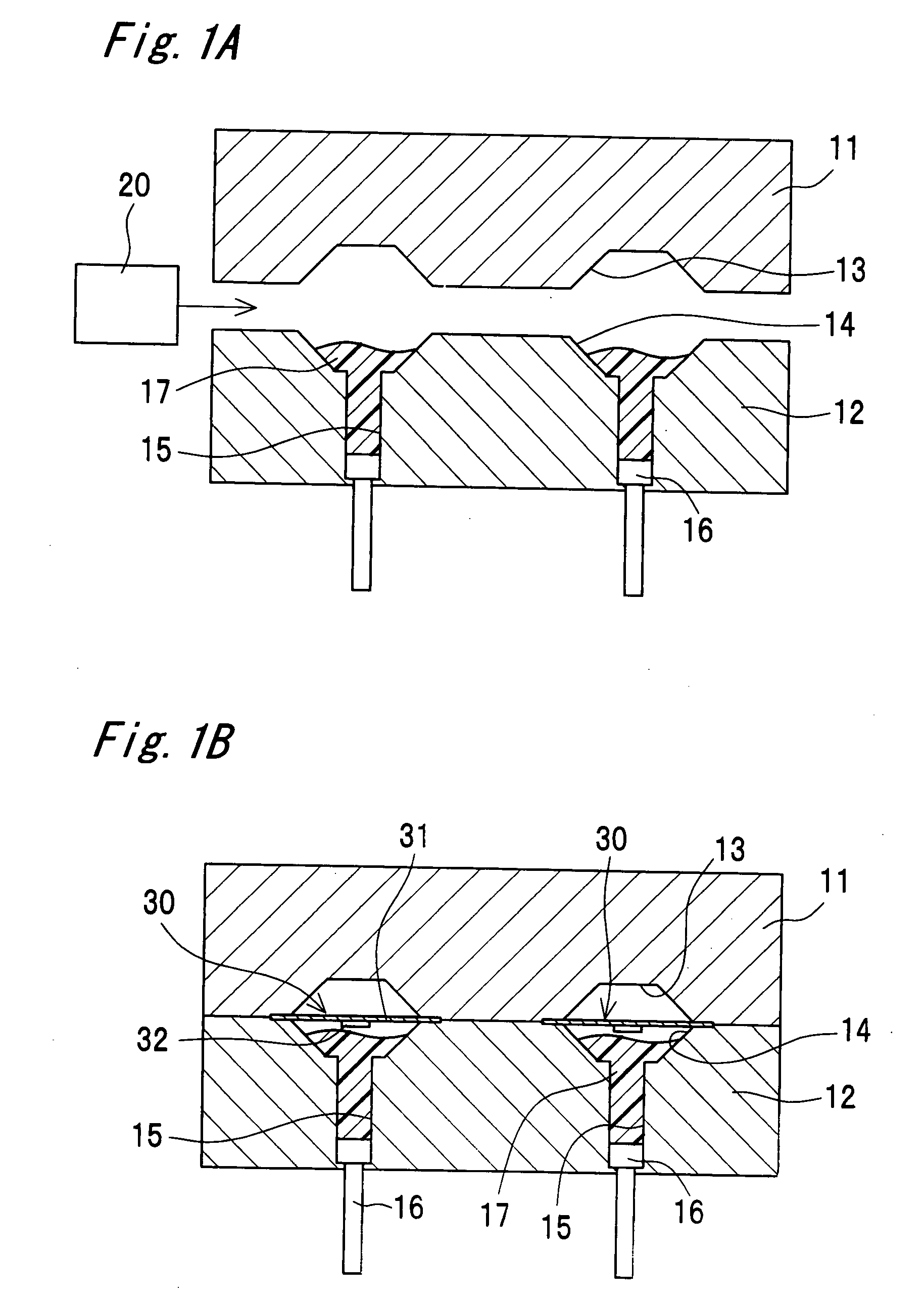
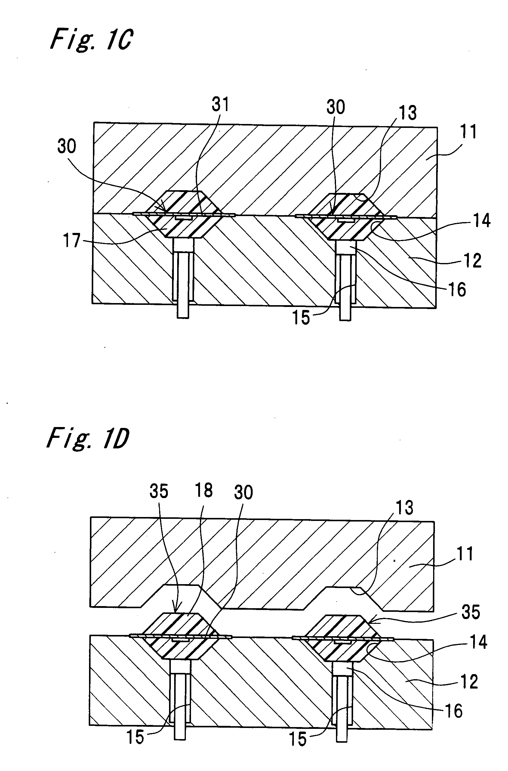
[0119]FIG. 1A shows a longitudinal sectional view of a semiconductor device manufacturing apparatus according to one embodiment of the present invention. The manufacturing apparatus has an upper metal mold 11, a lower metal mold 12 that relatively moves close to and away from the upper metal mold 11, and a filling device 20 that fills a space between the upper metal mold 11 and the lower metal mold 12 with a liquid-state resin 17.

[0120]The upper metal mold 11 has a plurality of cavities 13. The lower metal mold 12 has a plurality of cavities 14 and a resin reservoir hole 15 connected directly to each of the cavities 14. An injection member 16 is placed in the resin reservoir hole 15 so as to reciprocate therein.

[0121]The filling device 20 fills the cavities 14 and the resin reservoir hole 15 in the lower metal mold 12 with use of the liquid-state resin 17. The resin 17 is, for example, epoxy resin or silicone resin.

[0122]The upper metal mold 11 and the lower metal mold 12 cooperate ...

second embodiment

[0133]FIG. 2A shows a semiconductor device manufacturing apparatus according to a second embodiment of the present invention. The second embodiment is different from the first embodiment in construction of the filling device.

[0134]As shown in FIG. 2A, a filling device 21 of the second embodiment has a filling jig 22 and an opening and shutting device 25. The filling jig 22 has a jig main body 23 and a gate section 24. In the jig main body 23, resin injection holes 23a are formed. The gate section 24 openably closes the resin injection holes 23a. The resin injection holes 23a are filled with the liquid-state resin 17. Holes 24a are formed in the gate section 24. The opening and shutting device 25 moves the gate section 24 so that the holes 24a of the gate section 24 are aligned with the resin injection holes 23a of the jig main body 23, so as to open the resin injection holes 23a.

[0135]A method for filling the resin 17 by the filling device 21 is described next.

[0136]As shown in FIG...

third embodiment

[0139]FIG. 3 shows a semiconductor device manufacturing apparatus according to a third embodiment of the present invention. The third embodiment is different from the first embodiment in construction of the filling device.

[0140]As shown in FIG. 3, a filling device 26 of the third embodiment has a syringe-shaped resin feeder 27 and a tube 28 that extends from the resin feeder 27. The resin feeder 27 is filled with the liquid-state resin 17. Openings 28a are formed in the tube 28.

[0141]A method for filling the resin 17 by the filling device 26 is described next.

[0142]The tube 28 is placed on the lower metal mold 12 in such a way that the openings 28a of the tube 28 are aligned with the cavities 14 of the lower metal mold 12. At this time, the tube 28 is inserted and fixed between the upper metal mold 11 and the lower metal mold 12.

[0143]Then, the cavities 14 and the resin reservoir holes 15 are filled with the resin 17 through the openings 28a of the tube 28 from the resin feeder 27.

[...


PUM

PropertyMeasurementUnit
temperatureaaaaaaaaaa
shapeaaaaaaaaaa
diameteraaaaaaaaaa

Abstract

A semiconductor device manufacturing method includes the steps of filling a cavity and a resin reservoir hole in a lower metal mold with a liquid-state resin, holding a semiconductor element between the lower metal mold and an upper metal mold, injecting the resin in the resin reservoir hole into the cavity to seal the semiconductor device with the resin. Thus, the semiconductor device having almost no voids and less material loss is manufactured with high accuracy.

Description

CROSS-REFERENCE TO RELATED APPLICATION[0001]This nonprovisional application claims priority under 35 U.S.C. §119(a) on Patent Application No. 2006-032320 filed in Japan on 9 Feb. 2006 and Patent Application No. 2006-317300 filed in Japan on 24 Nov. 2006, the entire contents of which are incorporated herein by reference.BACKGROUND OF THE INVENTION[0002]The present invention relates to a semiconductor device manufacturing method and a semiconductor device manufacturing apparatus.[0003]In general, according to a method for manufacturing a semiconductor device, as shown in FIG. 15A, a semiconductor element 105 is manufactured by first bonding a semiconductor chip 102 to a lead frame 101 with an adhesive such as a silver paste. Then, as shown in FIG. 15B, the semiconductor chip 102 is connected to the lead frame 101 with a gold wire 103. Then, as shown in FIG. 15C, a semiconductor device 106 is manufactured by sealing the semiconductor element 105 with a resin 104. Subsequently, the semi...

Claims


Application Information

Patent Timeline
Patent Type & Authority Applications(United States)
IPC IPC(8): H01L33/00H01L29/24H01L21/56
CPCB29C39/10B29C39/24H01L2224/45144H01L2924/01079H01L2924/01078H01L2224/48465H01L2224/48247H01L2224/48091H01L33/54H01L33/52B29C45/14639B29C45/02H01L2924/00014H01L2924/00
Inventor TAKAKURA, HIDEYA
Owner SHARP KK
Why Eureka
Try Eureka