Rigid-flexible board and method for manufacturing the same

a rigid-flexible board and manufacturing method technology, applied in the direction of printed circuit manufacturing, printed circuit aspects, chemistry apparatus and processes, etc., can solve the problems of many processes, deterioration of the yield ratio of the board, and inability to obtain high productive yield, etc., to achieve low deformation, reduce the size variation, and simplify the manufacturing process of the rigid-flexible board

Inactive Publication Date: 2010-10-19
DAI NIPPON PRINTING CO LTD
View PDF28 Cites 14 Cited by
  • Summary
  • Abstract
  • Description
  • Claims
  • Application Information

AI Technical Summary

Benefits of technology

[0025]The conductive bump to be used as the vertical wiring area of the rigid board and the flexible board, and the connector of the flexible board is normally formed on the conductive metal layer. As the conductive metal layer, a conductive sheet such as electrolytic copper foil can be exemplified. The conductive sheet can be used by itself and patterned in a given shape. The shape of the conductive layer is not restricted. The conductive bump may be formed on one side or both sides. The conductive bump is made from conductive powders such as Ag, Au, Cu, solder powders, metallic alloy powders thereof or complex (mixed) metallic powders thereof, and a binder (e.g., polycarbonate resin, polysulfone resin, polyester resin, phenoxy resin, phenol resin, polyimide resin). As a result, the conductive bump is made from the conductive compound or conductive metal thereof. In the formation of the conductive bump from the conductive compound, the aspect ratio of the conductive bump can be increased by means of printing using a thicker metal mask. The height of the bump is generally set within a range of 100-400 μm. Moreover, the height of the bump can be determined in view of one synthetic resin sheet or some synthetic resin sheet. The conductive bump can be made of the conductive metal as follows. (a) Small metallic clusters with the same size or shape are dispersed on the conductive metal layer with an adhesive layer and selectively adhered (in this case, a mask may be used). (b) A plated resist is printed and patterned on the electrolytic copper foil and such a material as Cu, Sn, Au, Ag, solder is plated over the patterned resist to selectively form the small metallic column (bump). (c) A solder resist is coated and patterned on the conductive metal layer and the conductive metal layer with the patterned solder resist is immersed-into a soldering bath to form a small metallic column (bump). (d) A resist is formed so as to partially cover the metal plate to form a small metallic column (bump) through etching. Herein, the small metallic clusters and the small metallic column corresponding to the bump can be formed in a multilayered structure made of different materials or a multilayered shell structure. For example, an Au or Ag layer is coated on the Cu core so as to apply anti-oxidization characteristic to the bump. Also, a solder layer is coated on the Cu core so as to apply soldering connection to the bump. In the present invention, if the conductive bump is made from the conductive compound, the forming process of the bump can be simplified in comparison with the forming process using plating. Therefore, the manufacturing cost of the rigid-flexible board can be lowered.
[0027]In the present invention, when the synthetic resin sheets are applied on the conductive metal layers with the conductive bumps to form a plurality of laminated bodies, which are combined through heating and pressing, as the base (supporting member) for the synthetic resin sheets, a metal plate or a synthetic resin sheet-with lower size variation and lower deformation such as stainless steel, brass steel, polyimide resin plate (sheet) or polytetrafluoroethyrene resin plate (sheet) can be used.
[0028]According to the rigid-flexible board of the present invention, the rigid board and the flexible board are made independently and then, combined with one another. Therefore, the intended rigid-flexible board can be easily made. In this point of view, the manufacturing process for the rigid-flexible board can be simplified remarkably. Then, the rigid board and the flexible board can be formed into the finally desired shapes before the combination. Therefore, the connecting area of the rigid board may not be punched out previously and the connecting area of the flexible board may not be punched out previously so that the material yield efficiency can be enhanced through the lowering the waste material. Then, since the rigid board and the flexible board can be detected in defect under the condition of the finally desired shapes, the material loss relating to the boards can be lowered even though some defects are detected during the formation process of the boards.
[0029]In the present invention, the rigid board includes a step for connecting the rigid board with the flexible board. In this case, since the flexible board is connected to the rigid board via the step, the main surface level of the flexible board can be substantially equal to or lower than the main surface level of the rigid board so that the main surface of the flexible board can not disturb the component mounting process. In the case of screen-printing solder cream onto a component mounting surface, if the main surface level of the flexible board is higher than the main surface level of the rigid board, the screening surface for printing is contacted with the flexible board and thus, not contacted with the rigid board. Therefore, the screen printing can not be performed under good condition. If the main surface level of the flexible board is equal to or lower than the main surface level of the rigid board, the above-mentioned disadvantage can be removed. Normally, however, if the solder resist film is formed in a thickness of 20-50 μm on the rigid board, the screen printing can be carried out without the above-mentioned disadvantage. Moreover, if the solder resist is formed apart from the solder cream printing pattern, the solder resist film with even a thickness of 100 μm can not disturb the above-mentioned screen printing. Herein the phrase of “the main surface level of the flexible board being equal to or lower than the main surface level of the rigid board” means that the screen printing can be performed not subject to the solder resist film, and thus, can be defined normally as 100 μm or below, preferably as 50 μm or below.

Problems solved by technology

As described above, in the conventional manufacturing method of rigid-flexible board, since the flexible board is formed between the adjacent rigid boards (particularly, the main surface level of the flexible board is substantially equal to or lower than the main surface level of the rigid board), complicated many processes are required.
In this case, much waste is created from the punched out portions so that the yield ratio of the boards is deteriorated.
Then, since a plurality of rigid-flexible board units are formed in the large board, if one of the synthetic resin sheets or one of the rigid-flexible board units is failed, all of the rigid-flexible board units are failed so that high productive yield can not be obtained.

Method used


Image

  • Rigid-flexible board and method for manufacturing the same
  • Rigid-flexible board and method for manufacturing the same
  • Rigid-flexible board and method for manufacturing the same

Examples


Embodiment Construction

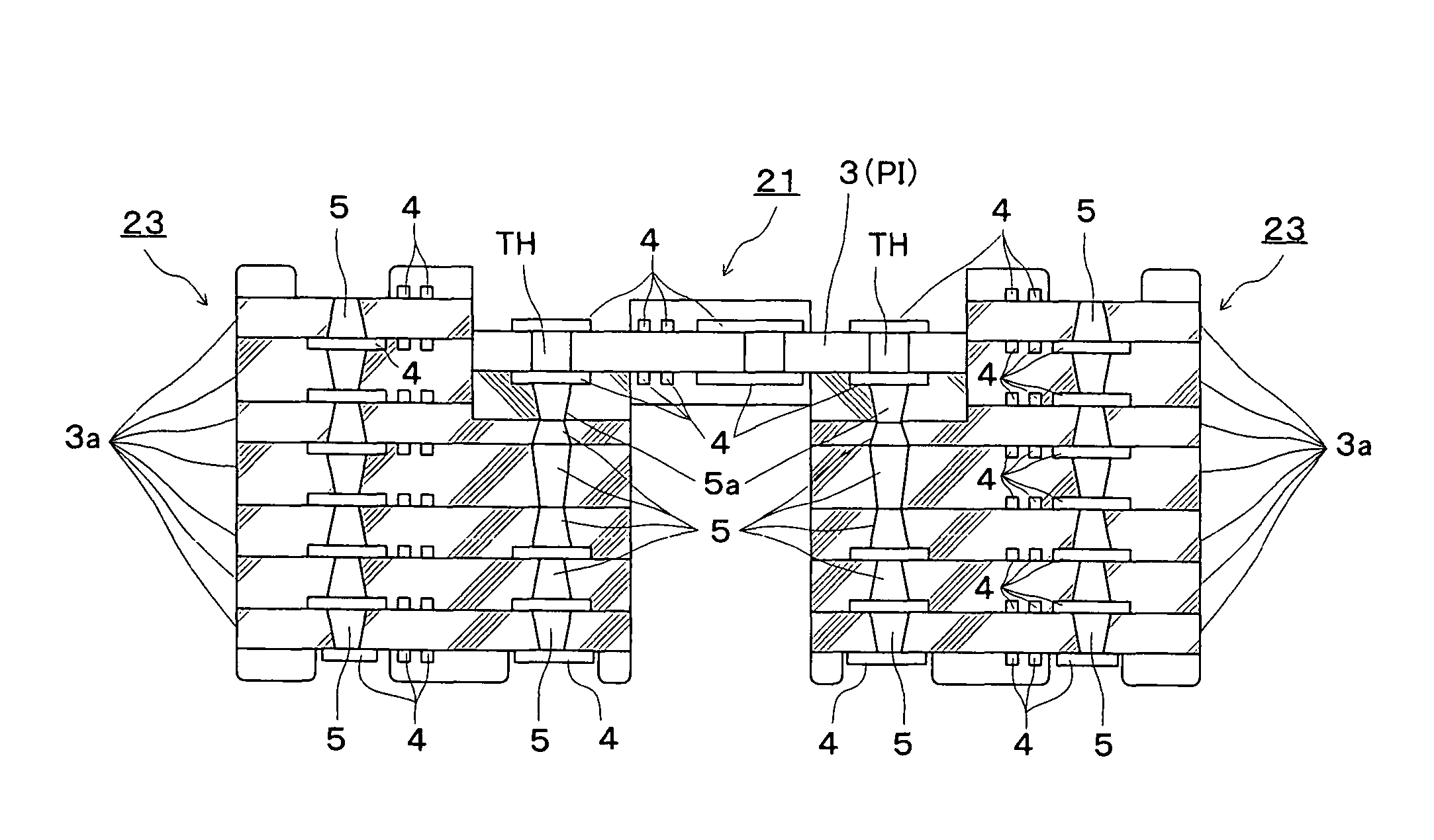
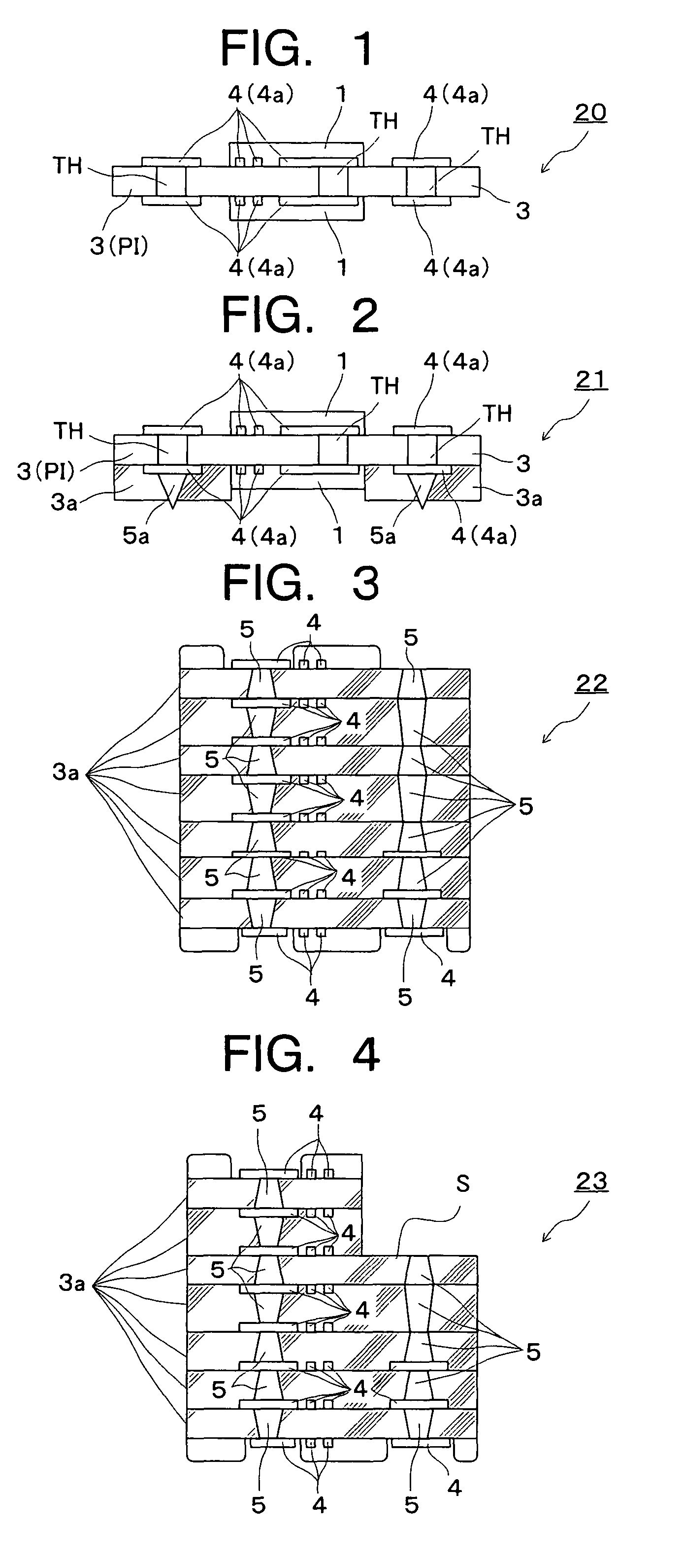
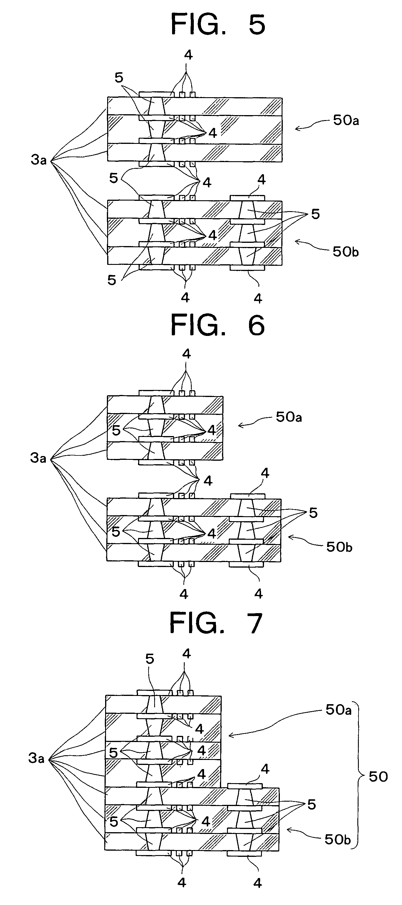
[0054]An embodiment according to the present invention will be described with reference to the FIGS. 1-16. In this case, the same references are imparted to like components through FIGS. 1-16 and 17-23 so that the explanation for like components will be omitted.

(Formation of Flexible Board)

[0055]First of all, electrolytic copper foils 4a with a thickness of 18 μm are applied on the both main surfaces of the polyimide film 3(PI) with a thickness of 25 μm to form a flexible board with copper foils on both of the main surfaces wherein through holes (TH) are formed at predetermined positions of the board.

[0056]Then, a normal resist ink for etching (trade name: PSR-4000H made by Taiyo Ink Mfg Co., Ltd) is screen-printed on the electrolytic copper foils 4a of the flexible board. After the conductive patterned area is masked with resist, the electrolytic copper foils 4a are etched with an etching solution of copper chloride, and the resist mask is removed so as to form a two-sided flexible...


PUM

PropertyMeasurementUnit
heightaaaaaaaaaa
thicknessaaaaaaaaaa
thicknessaaaaaaaaaa

Abstract

A rigid-flexible board and a method for manufacturing the same can be provided, whereby the material yield ratio can be enhanced and the productive yield can be also enhanced. A rigid board with a step for connection and a flexible board with a connector at the edge thereof are formed independently. Then, the connecting area is spot facing processed so that the depth of the thus obtained depressed portion is equal to or lower than the thickness of the flexible board. The connector of the flexible board is electrically connected to the vertical wiring area of the depressed portion.

Description

TECHNICAL FIELD[0001]The present invention relates to a method for manufacturing a rigid-flexible board, particularly comprising a plurality of rigid boards which are connected to a flexible board so that the main surface level of the flexible board is equal to or lower than the main surface levels of the rigid board.BACKGROUND ART[0002]In disposing a rigid board over a bending portion of a steel case, generally, the rigid board is divided into a plurality of pieces which are to be connected with one another by utilizing connectors or a flexible board.[0003]In the connecting the rigid board pieces with the connectors or the flexible board, however, the thickness of the thus obtained assembly is increased by the thickness of the connectors or the flexible board so as to prevent the thinning of the intended instrument. Moreover, after the rigid board pieces are connected with the connectors or the flexible board, the same treatment and processing can not be carried out for the rigid b...

Claims


Application Information

Patent Timeline
Patent Type & Authority Patents(United States)
IPC IPC(8): H01R12/00H05K1/02H05K1/14H05K3/00H05K3/36H05K3/46
CPCH05K3/4691H05K3/0052H05K3/4614H05K3/462H05K2201/0187H05K2201/0919H05K2201/096H05K2201/09845H05K2203/0169H05K2203/061H05K3/46
Inventor KOBAYASHI, ATSUSHIUMEDA, KAZUOGOTOU, WATARUNAKAZAWA, SUSUMUTAKEUCHI, KIYOSHITERAUCHI, TAKAYUKI
Owner DAI NIPPON PRINTING CO LTD
Why Eureka
Try Eureka