Plasma display panel and method of manufacturing the same

a technology of plasma display panel and magnesium oxide, which is applied in the manufacture of electrode systems, cold cathode manufacturing, and electric discharge tube/lamp manufacture, etc., can solve the problems of short circuit of electrodes, low power consumption of plasma display panel including the protective layer made of magnesium oxide, and low firing voltage. , to achieve the effect of improving secondary electron emission characteristics, low power consumption and low firing voltag

Inactive Publication Date: 2007-08-09
LG ELECTRONICS INC
View PDF0 Cites 0 Cited by
  • Summary
  • Abstract
  • Description
  • Claims
  • Application Information

AI Technical Summary

Benefits of technology

[0014] An object of the present invention is to provide a plasma display panel having improved secondary electron emission characteristics, and thus, low firing voltage and low power consumption.
[0015] Another object of the present invention is to provide a plasma display panel and a method of forming the plasma display panel wherein the yield of VUV rays generated during the discharge is increased, whereby the brightness and the luminous efficiency of the plasma display panel are improved.

Problems solved by technology

At this time, short circuits of the electrodes may be caused by metal elements such as sodium (Na).
However, the plasma display panel as described above according to the related art has the following problems and limitations.
Firstly, although the protective layer including magnesium oxide of the plasma display panel may sufficiently withstand the bombardment of positive (+) ions, the protective layer does not effectively lower the discharge voltage.
This limitation is caused by the physical characteristics of magnesium oxide, which is a principal material for the protective layer.
However, the power consumption of the plasma display panel including the protective layer made of magnesium oxide still remains high.
For this reason, there has been much research on a substitute for the magnesium oxide as a material for the protective layer, but there has not been yet proposed positively verified materials due to reliability problems thereof.
Thirdly, vacuum ultraviolet (VUV) rays are emitted from a discharge space in arbitrary directions at the time of discharge of the plasma display panel.
This limitation then lowers the power usage efficiency of the plasma display panel and the display quality of the plasma display panel.

Method used


Image

  • Plasma display panel and method of manufacturing the same
  • Plasma display panel and method of manufacturing the same
  • Plasma display panel and method of manufacturing the same

Examples


first embodiment

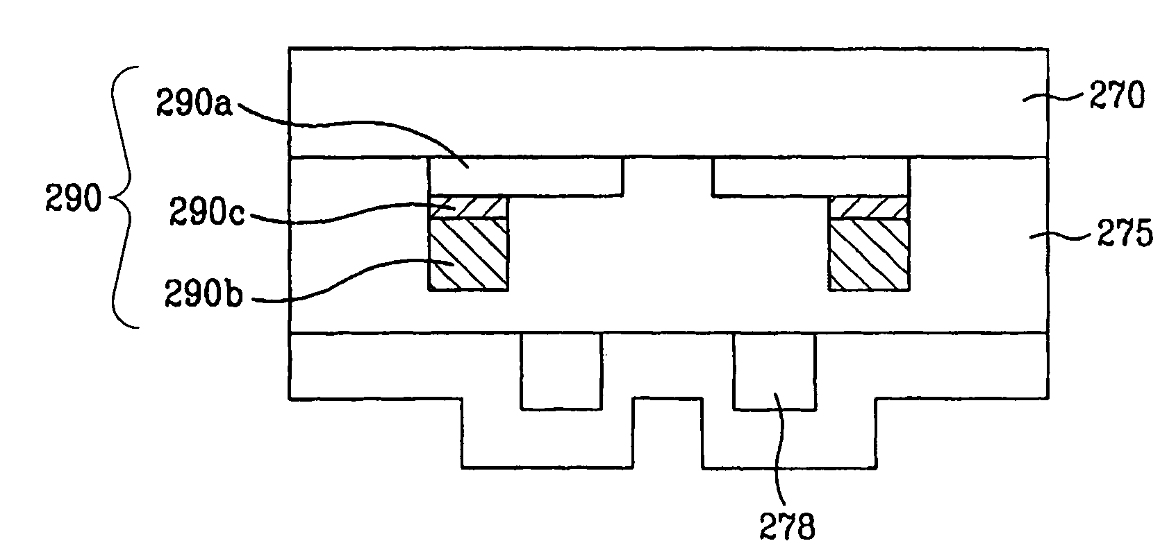
[0038]FIG. 2 is a view illustrating a plasma display panel according to the present invention. Particularly, the upper panel of the plasma display panel is shown, but the plasma display panel includes other components including the lower panel, barrier ribs, phosphors, etc. The lower panel can have the structure as shown in FIG. 9.

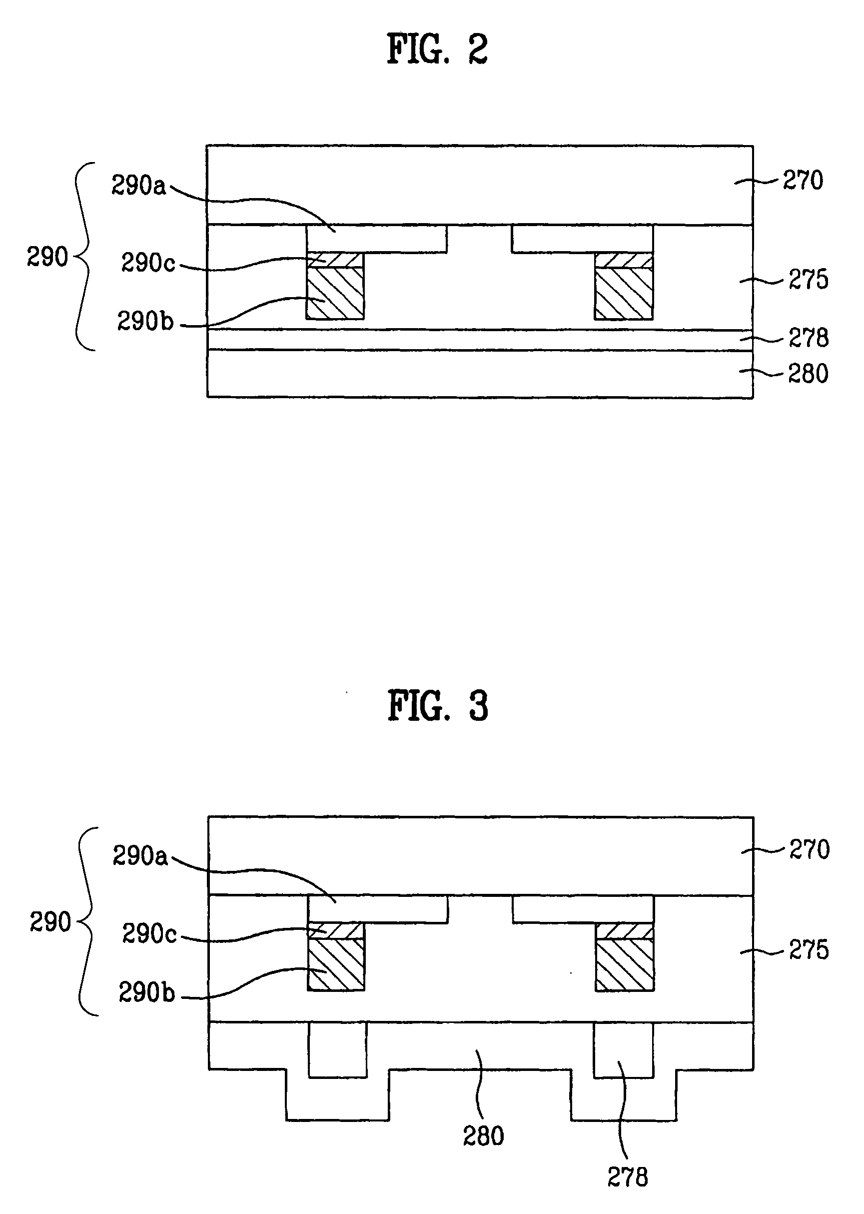
[0039] As shown in FIG. 2, the upper panel of the plasma display panel includes one or more sustain electrode pairs 290 (290a, 290b) formed on an upper substrate 270, an upper dielectric layer 275 formed on the sustain electrode pair(s) 290, and a protective layer 280 formed on the upper dielectric layer 275. Each sustain electrode pair 290 includes a transparent electrode 290a and a bus electrode 290b on the transparent electrode 290a. Optionally, a black electrode 290c may be interposed between the transparent electrode 290a and the bus electrode 290b. In fact, in all embodiments (e.g., FIGS. 2-10) described herein, the bus electrode 290b may be formed d...

second embodiment

[0043] Referring to FIG. 3, the VUV reflecting layer 278 is formed on the upper dielectric layer 275 at positions corresponding to the bus electrodes 290b. For instance, the VUV reflecting layer 278 in the form of projections is formed on the dielectric layer 275, and the projections (VUV reflecting layer 278) are aligned or substantially aligned with the bus electrodes 290b as shown.

third embodiment

[0044] Referring to FIG. 4, the VUV reflecting layer 278 is formed on the upper dielectric layer 275 at positions corresponding to transparent electrodes 290a. For instance, the VUV reflecting layer 278 in the form of projections is formed on the dielectric layer 275, and the projections (VUV reflecting layer 278) are aligned or substantially aligned with the transparent electrodes 290a as shown.


PUM


Abstract

A plasma display panel having improved luminous efficiency is disclosed. The plasma display panel according to an embodiment of the present invention includes a first panel and a second panel. The first panel has an ultraviolet (UV) reflecting layer formed therein.

Description

CROSS-REFERENCE TO RELATED APPLICATION [0001] This application claims the priority benefit of Korean Patent Application No. 10-2006-0002212 filed on Jan. 9, 2006 and Korean Patent Application No. 10-2006-0003193 filed on Jan. 11, 2006, which are hereby incorporated by reference in its entirety as if fully set forth herein. BACKGROUND OF THE INVENTION [0002] 1. Field of the Invention [0003] The present invention relates to a plasma display panel, and more particularly, to improvement of the luminous efficiency of a plasma display panel. [0004] 2. Discussion of the Related Art [0005] Generally, a plasma display panel comprises an upper panel, a lower panel, and barrier ribs formed between the upper and lower panels to define respective discharge cells. The respective discharge cells are filled with a major discharge gas, such as neon, helium, or a mixed gas of neon and helium, and with an inert gas containing a small amount of xenon (Xe). When a high-frequency voltage is applied to th...

Claims


Application Information

Patent Timeline
Patent Type & Authority Applications(United States)
IPC IPC(8): H01J17/49
CPCH01J9/02H01J11/44H01J11/38H01J11/12
Inventor KIM, BO HYUNPARK, MIN SOOPARK, DEOK HAIRYU, BYUNG GILKIM, YOUNG SUNG
Owner LG ELECTRONICS INC
Why Eureka
Try Eureka