
Developing apparatus and developing method

Active Publication Date: 2007-08-09
SCREEN HLDG CO LTD
View PDF12 Cites 29 Cited by
  • Summary
  • Abstract
  • Description
  • Claims
  • Application Information

AI Technical Summary

Benefits of technology

[0015] This invention has been made having regard to the state of the art noted above, and its object is (I) to provide a developing apparatus and a developing method that can prevent generation of post-develop defects due to a large angle of contact of substrates, and (II) to provide a developing apparatus and a developing method for developing substrates in a reduced time.

Problems solved by technology

Moreover, considering the resist to be used in immersion exposure expected to be implemented in the near future, the angle of contact is likely to become still larger.
When the angle of contact of the substrate becomes large, there arises an inconvenience that the substrate cannot not be dried effectively.
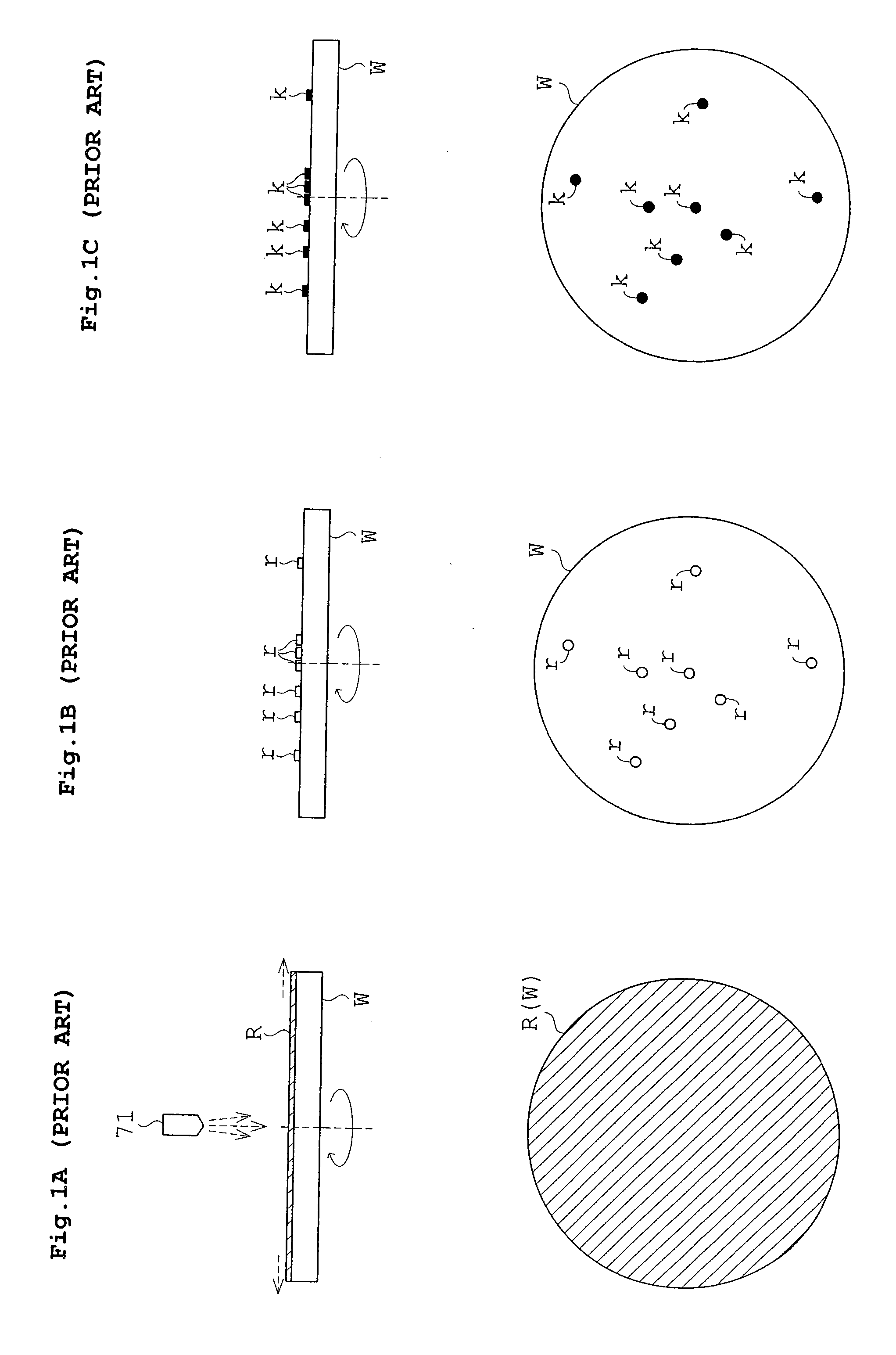
When the droplets “r” of the rinsing liquid are sufficiently small, the centrifugal force produced by the spinning wafer W may fail to act on the droplets “r” of the rinsing liquid, thereby allowing the droplets “r” to remain on the wafer W. The components of the resist will dissolve in the droplets “r” of the rinsing liquid remaining on the wafer W. This results in an inconvenience that, as shown in FIG. 1C, the components of the resist dissolved in the droplets “r” of the rinsing liquid form deposits, which become post-develop defects “k”, on the wafer W having undergone a drying process.
The conventional method and apparatus have a drawback of requiring a long time for developing substrates.
Since a long time is required for development, it is difficult to achieve a further improvement in the throughput of the developing apparatus.
To increase the number of developing units in order to improve the throughput of the developing apparatus is unrealistic from the viewpoint of cost and footprint

Method used


Image

  • Developing apparatus and developing method
  • Developing apparatus and developing method
  • Developing apparatus and developing method

Examples


Embodiment Construction

[0053] A preferred embodiment of this invention will be described in detail hereinafter with reference to the drawings.

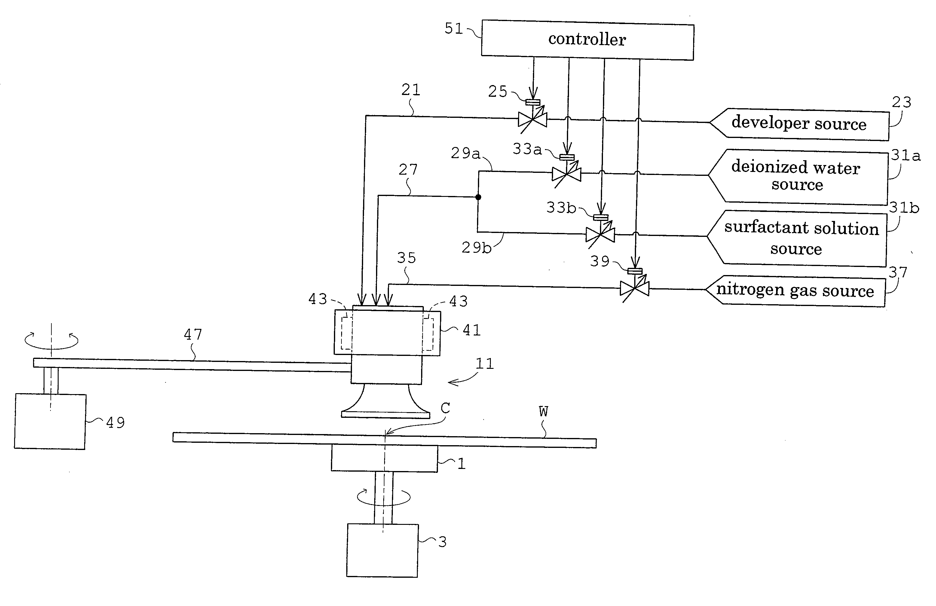
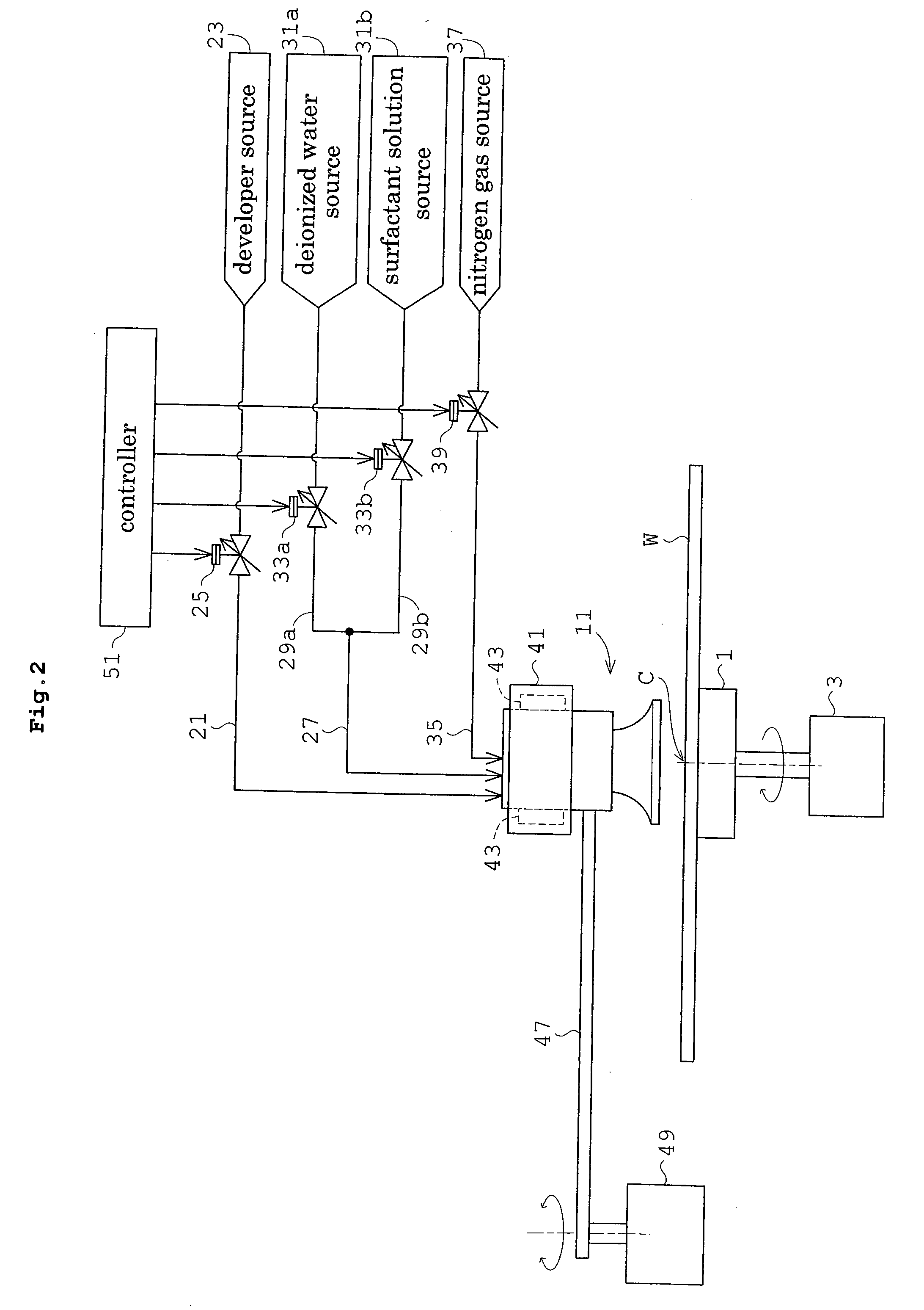
[0054]FIG. 2 is a view showing an outline of a developing apparatus according to this invention. FIG. 3A is a view in vertical section of a joint nozzle 11. FIG. 3B is a view in cross section of the joint nozzle 11.

[0055] The developing apparatus includes a spin chuck 1 for supporting, by suction, the lower surface of a wafer W in horizontal posture. The spin chuck 1 has a vertical output shaft of a first motor 3 connected to the lower end thereof. The first motor 3 spins the wafer W at a predetermined rotational frequency. At this time, the wafer W has a spin center C located on an extension of the output shaft of the first motor 3. The spin chuck 1 and first motor 3 correspond to the spin-support device in this invention.

[0056] The spin chuck 1 is surrounded by a cup (not shown) for collecting deionized water, a developer and so on scattering from the wafer W. ...


PUM


Abstract

A joint nozzle that delivers a developer, a rinsing liquid and nitrogen gas is disposed adjacent the spin center of a substrate in plan view. A controller operates electromagnetic switch valves to continue supply of the developer, while spinning the substrate, in a developing process, and to start supply of the rinsing liquid in a rinsing process, immediately after the supply of the developer ends, thereby achieving a shortened period of the developing process. A switching is made to a drying process by starting supply of the nitrogen gas immediately after completion of the rinsing process. Thus, even if the substrate has a large angle of contact, formation of droplets of the rinsing liquid is inhibited to prevent post-develop defects.

Description

BACKGROUND OF THE INVENTION [0001] (1) Field of the Invention [0002] This invention relates to a developing apparatus and development method for developing semiconductor wafers, glass substrates for photomasks, glass substrates for liquid crystal displays and flat panel displays, and substrates for optical disks (hereinafter called simply “substrates”). [0003] (2) Description of the Related Art [0004] As one of the methods of developing resist film formed on surfaces of substrates, a puddle development mode is used widely (as disclosed in Japanese Unexamined Patent Publication No. 2003-109894, for example). This developing mode may be divided broadly into a developing process, a rinsing process and a drying process as described below. [0005] First, a developer is supplied while moving a developer nozzle relative to a substrate, to form a puddle of the developer on the substrate. In this state, the substrate is maintained still for a predetermined period to allow for progress of a de...

Claims


Application Information

Patent Timeline
IPC IPC(8): G03D5/00
CPCG03F7/3021H01L21/67253H01L21/67051
Inventor MITSUHASHI, TSUYOSHISUGIMOTO, KENJI
Owner SCREEN HLDG CO LTD
Learn More