Developing device and developing method

a technology of developing device and developing method, which is applied in the direction of liquid/solution decomposition chemical coating, instruments, photosensitive materials, etc., can solve the problems of dissolved resist components that begin to exhibit adverse effects and diffuse dissolved resist components forcibly, and achieve uniform line width

Inactive Publication Date: 2007-08-09
TOKYO ELECTRON LTD
View PDF5 Cites 25 Cited by
  • Summary
  • Abstract
  • Description
  • Claims
  • Application Information

AI Technical Summary

Benefits of technology

[0006] The present invention has been made in view of the problems. It is, therefore, an object of the present invention to provide a developing apparatus and method capable of forming a pattern having a uniform line width by avoiding the influence of the dissolved resist components, even when various types of resists having different dissolution rates are developed.
[0009] Delivering the diluent at an appropriate timing after supplying the developing solution, the progress of the development reaction is suppressed or stopped. Further, the delivery of the diluent generates a flow in a liquid film on the substrate, causing the dissolved resist components to diffuse forcibly. As a result, it is possible to prevent variations in the line width and development defects occurring as a result of the dissolution of the resist being locally promoted or delayed due to the uneven distribution of the dissolved resist components. The diluent is preferably supplied to the developing solution on the substrate, after the bottom portion of the resist has been dissolved such that a desired line width is achieved, but before the dissolved resist components begin to exhibit adverse effect due to increase in their concentration.
[0010] In one preferred embodiment of the present invention, a plurality of developer supply nozzles are prepared; and a temperature regulating unit is assigned to each developer supply nozzle to control the temperature of the developing solution to be supplied by the developer supply nozzle. While the substrate is being processed by using a first one of the developer supply nozzles, the temperature regulating unit for a second one of the developer supply nozzles adjusts the temperature of the developing solution for this nozzle. Thus, when processing substrates with resists that are required to be developed at different temperatures, the development of a substrate with a second type of resist performed by supplying a developing solution of a second temperature from the second developer supply nozzle can be started immediately after the completion of the development of a substrate with a first type of resist performed by supplying a developing solution of a first temperature from the first developer supply nozzle. Thus, a plurality of developing solutions may be set at different temperatures beforehand, and one of them may be selected and used based on the resist to be developed. This prevents situations where the time required to heat or cool the developing solution adversely affects the throughput of the developing apparatus.
[0011] The plurality of developer supply nozzles may be integrated together into a single liquid-supplying nozzle. That is, the term “plurality” of developer supply nozzles is not limited to a plurality of developer nozzles separated from each other. Use of the integrated liquid-supplying nozzle unit reduces the footprint of the developing apparatus. Furthermore, a single drive mechanism is enough to move the nozzle, resulting in a simplified configuration of the developing apparatus.
[0013] A developer supply nozzle and a diluent supply nozzle may be integrated together into a single liquid-supplying nozzle unit. This liquid-supplying nozzle unit may be configured to eject a developing solution and a diluent through a common ejection port. The integration of the developer supply nozzle and the diluent supply nozzle reduces the footprint of the developing apparatus and simplifies the configuration of the nozzle moving mechanism. The developer supply nozzle and the diluent supply nozzle may be provided separately. In such a case, the nozzle moving speed and the nozzle moving direction when ejecting a developing solution may be the same as those when ejecting a diluent.
[0014] The liquid-supplying nozzle unit formed by integrating the developer supply nozzle and the diluent supply nozzle together may be configured to eject a developing solution and a diluent through their respective separate ejection ports. In this case, the developer ejection port and the diluent ejection port may be disposed at the front side and the back side with respect to the direction of movement of the nozzle unit when supplying a liquid. When the developer ejection port is located in front of the diluent ejection port with respect to the moving direction of the nozzle unit when supplying the liquid, a suction port may be provided between these ejection ports to suck the liquid. When developing a resist that requires only a very short developing time, the nozzle unit may be moved while simultaneously ejecting a developing solution and a diluent through the developing solution ejection nozzle and the diluent ejection nozzle behind the developing solution ejection nozzle, respectively. In this case, sucking the liquid on the substrate through the suction port can prevent development defects due to disturbed flow occurring as a result of collision between the developing solution and the diluent.

Problems solved by technology

Further, the delivery of the diluent generates a flow in a liquid film on the substrate, causing the dissolved resist components to diffuse forcibly.
The diluent is preferably supplied to the developing solution on the substrate, after the bottom portion of the resist has been dissolved such that a desired line width is achieved, but before the dissolved resist components begin to exhibit adverse effect due to increase in their concentration.

Method used


Image

  • Developing device and developing method
  • Developing device and developing method
  • Developing device and developing method

Examples


Embodiment Construction

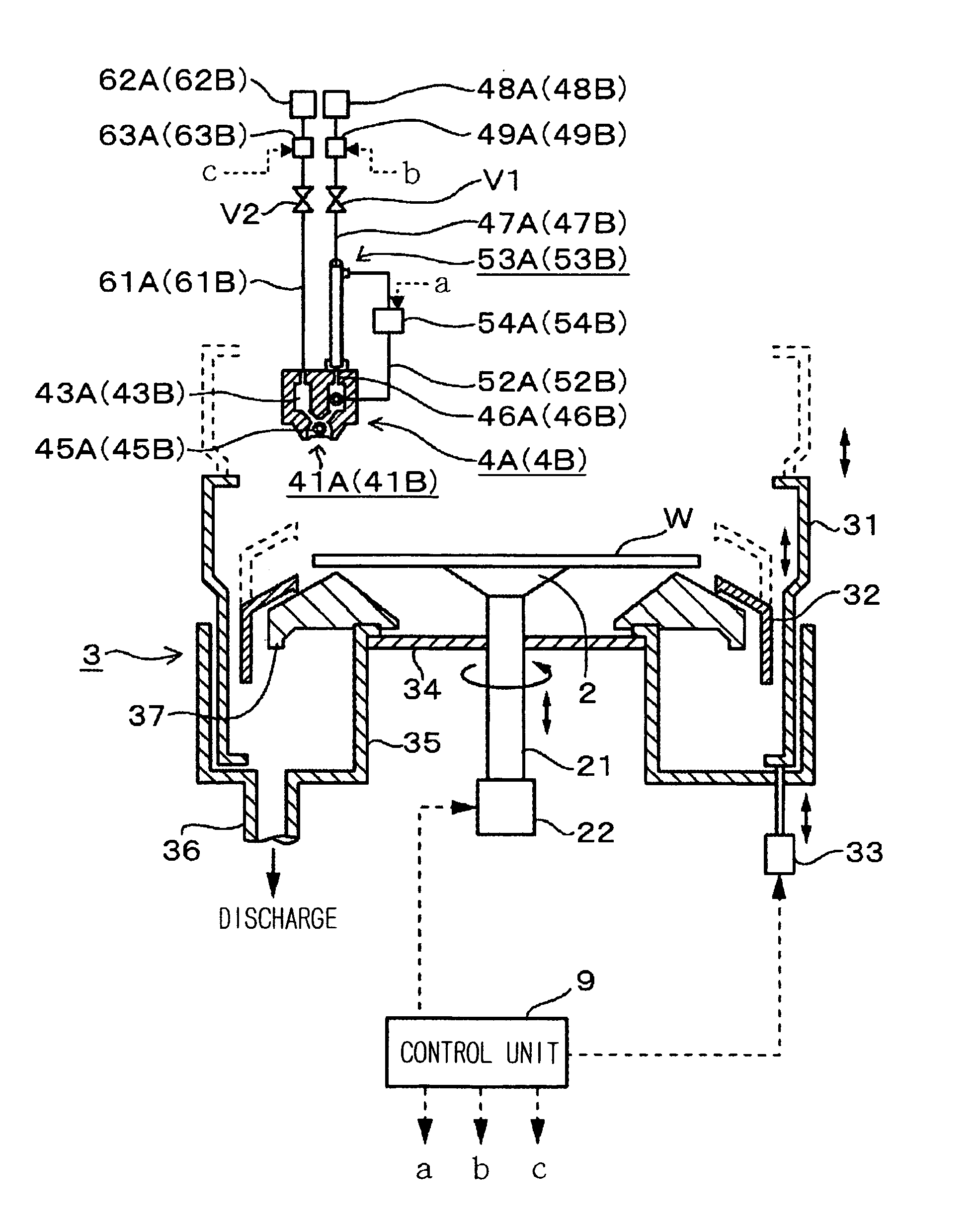
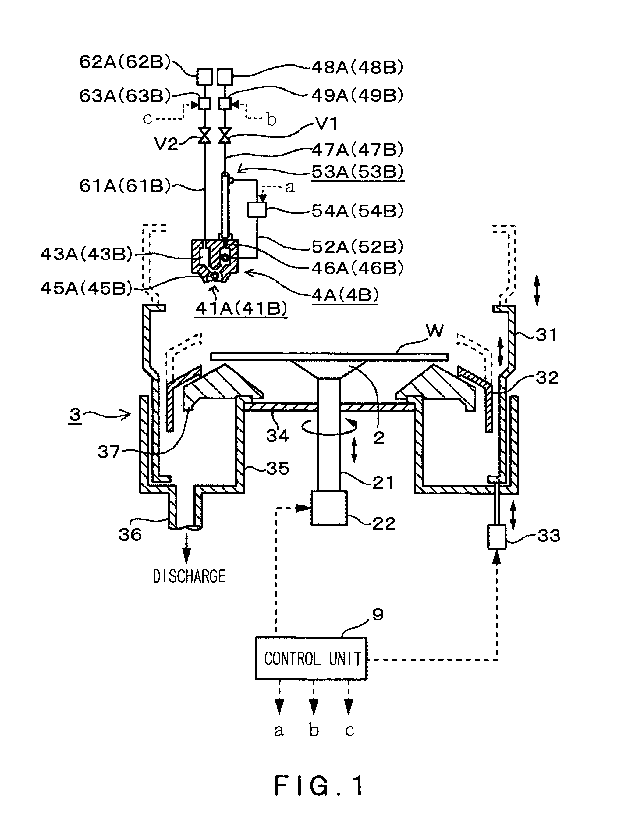
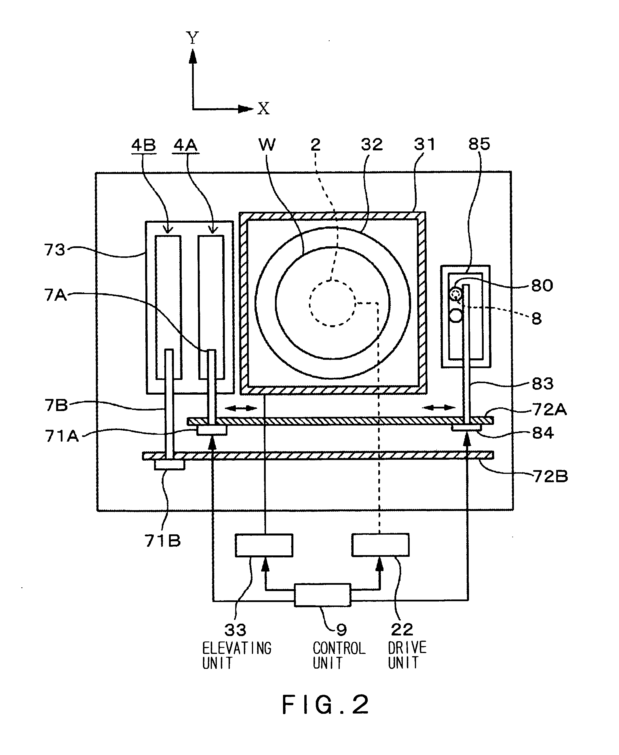
[0036] A developing apparatus in one embodiment of the present invention will be described with reference to FIGS. 1 and 2. Reference numeral 2 denotes a spin chuck (i.e., a substrate holding unit) for holding a substrate (e.g., a wafer W) in a horizontal attitude by holding the center portion of the back side of the substrate by suction. The spin chuck 2 is connected to a drive mechanism 22 through a rotational shaft 21 and can be rotated, raised and lowered together with the wafer W held thereon, by the drive mechanism 22.

[0037] A cup set 3 is provided so as to surround the wafer W held on the spin chuck 2. The cup set 3 comprises an inner cup 32 and an outer cup 31 each having an opened top end. The outer cup 31 has an upper portion thereof having a shape of a rectangular tube and a lower portion thereof having a cylindrical shape. The inner cup 32 has a shape of a cylinder having an upper portion thereof tapered inwardly. The outer cup 31 is raised and lowered by an elevating m...


PUM

PropertyMeasurementUnit
temperatureaaaaaaaaaa

Abstract

The temperature of a developing solution is varied depending on the type of resist or the resist pattern. The developing solution is applied while scanning a developer nozzle having a slit-shaped ejection port that has a length matching the width of the effective area of the substrate. After leaving the substrate with the developing solution being coated thereon for a predetermined period of time, a diluent is supplied while scanning a diluent nozzle, thereby substantially stopping the development reaction and causing the dissolved resist components to diffuse. A desired amount of resist can be quickly dissolved through the control of the developing solution temperature, while the development can be stopped before the dissolved resist components exhibit adverse effect through the supply of the diluent a predetermined timing, whereby achieving a pattern having a uniform line width and improved throughput.

Description

TECHNICAL FIELD [0001] The present invention relates to a developing apparatus and method for developing an exposed resist on a substrate surface. BACKGROUND ART [0002] A semiconductor manufacturing process includes a photoresist process in which a resist is coated onto the surface of a semiconductor wafer (hereinafter referred to simply as a wafer), exposed in a predetermined pattern, and then developed to form a resist pattern. Such a process is generally performed by a system in which a coating-and-developing apparatus for coating and developing a resist is connected to an exposure apparatus. [0003] The developing apparatus disclosed in JP2001-327909A includes a developer nozzle 11 having a slit formed in its underside and extending in the longitudinal direction thereof, as shown in FIG. 16. This slit acts as an ejection port and has a length equal to or larger than the diameter of the wafer (W). The developer nozzle 11 moves from one end to the opposite end of the wafer W, which...

Claims


Application Information

Patent Timeline
Patent Type & Authority Applications(United States)
IPC IPC(8): B05C11/00B05B7/06B05D1/02B05B3/00G03F7/30H01L21/027
CPCG03F7/3028G03F7/3021H01L21/6715
Inventor YAMAMOTO, TAROYOSHIHARA, KOUSUKEKYOUDA, HIDEHARUTAKEGUCHI, HIROFUMIOOKOUCHI, ATSUSHI
Owner TOKYO ELECTRON LTD
Why Eureka
Try Eureka