Position-dependent variation amount computation method and circuit analysis method

Inactive Publication Date: 2007-08-09
SOCIONEXT INC
View PDF6 Cites 61 Cited by
  • Summary
  • Abstract
  • Description
  • Claims
  • Application Information

AI Technical Summary

Benefits of technology

[0008]It is therefore an object of the present invention to makes it possible to calculate a variation amount depending on change of a position of a device and the like using layout position information of a semiconductor integr

Problems solved by technology

Moreover, when a plurality of parameters are intentionally distributed at random b

Method used


Image

  • Position-dependent variation amount computation method and circuit analysis method
  • Position-dependent variation amount computation method and circuit analysis method
  • Position-dependent variation amount computation method and circuit analysis method

Examples


first embodiment

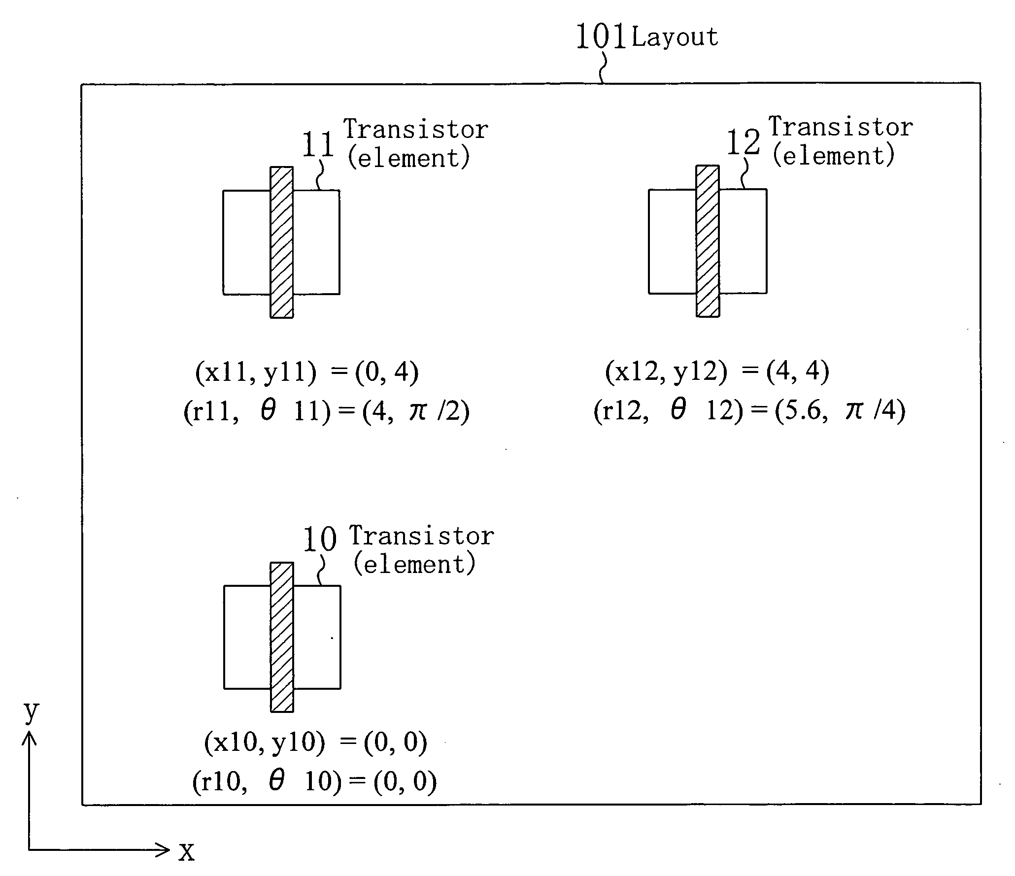
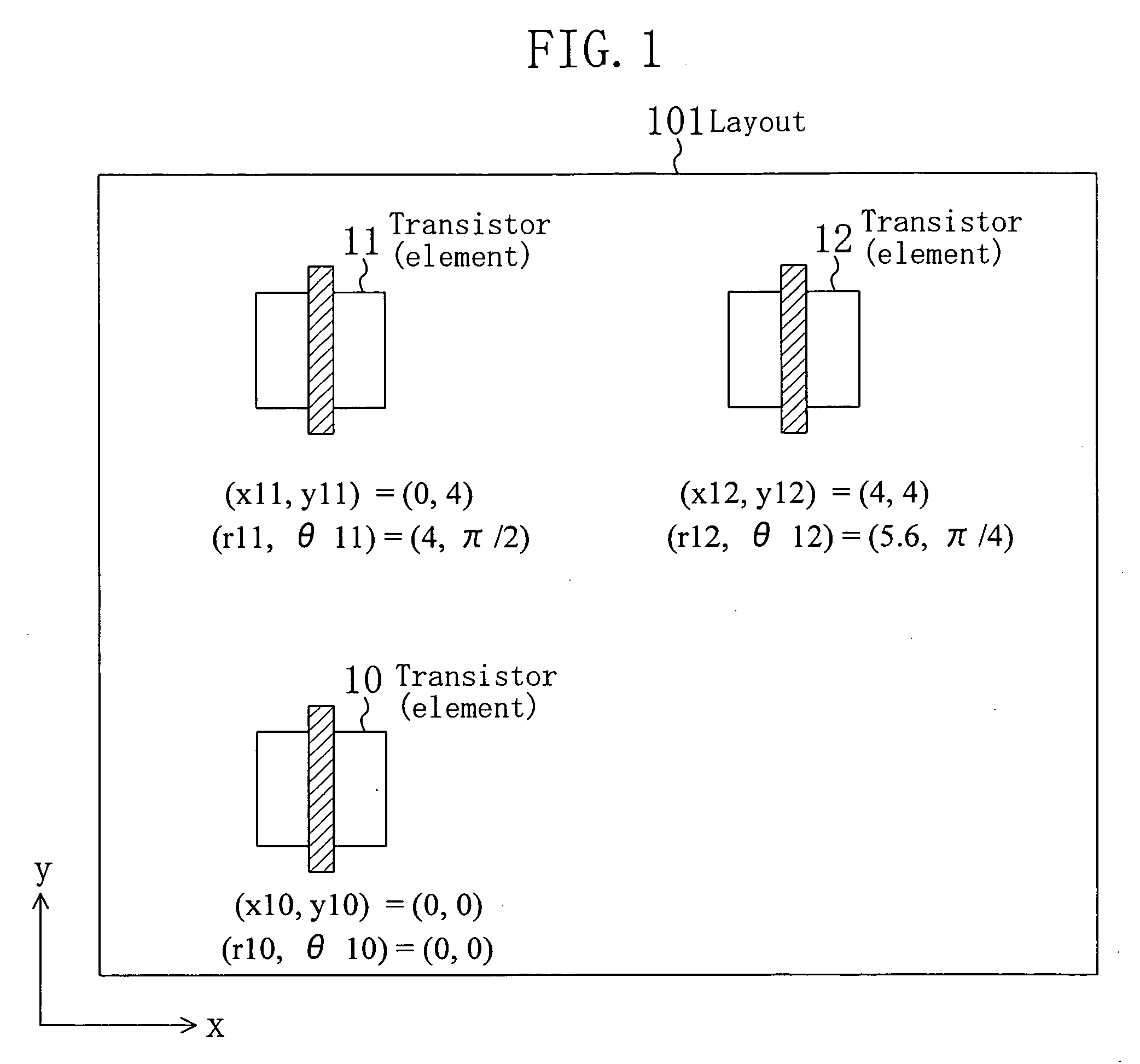
[0051]FIG. 1 is a diagram illustrating layout position information for each element in a semiconductor integrated circuit according to an embodiment of the present invention.

[0052]In FIG. 1, the reference numeral 101 denotes a layout of a semiconductor integrated circuit. FIG. 1 shows on-wafer or on-chip layout position information for each element constituting the semiconductor integrated circuit. In FIG. 1, as elements constituting the semiconductor integrated circuit, three transistors 10, 11 and 12 are arranged. Assume that respective arrangement positions of the transistors 10, 11 and 12 are expressed by positional coordinates of a Catesian coordinate system. Positional coordinates (x10, y10) of the transistor 10 are (0, 0), positional coordinates (x11, y11) of the transistor 11 are (0, 4) and positional coordinates (x12, y12) of the transistor 12 are (4, 4). Except for arrangement position, conditions for the three transistors 10, 11 and 12 are the same. For example, the trans...

second embodiment

[0070]A position-dependent variation amount computation method according to a second embodiment of the present invention will be described.

[0071]In this embodiment, the case where the gate width dimension difference ΔW for a gate width of a transistor has a distribution characteristic with a mean μw and a standard deviation μw will be described. In this case, each of a mean σw and a standard deviation σw of process variations for the gate width dimension difference ΔW is a position-dependent variation amount.

[0072]The mean μw and the standard deviation σw of process variations for the gate width dimension difference ΔW of a transistor are calculated using a position topology Zm and a position topology Zs, according to the following Equation 10 and Equation 11. The position topologies Zm and Zs are defined by the following Equation 12 and Equation 13, respectively.

μw=0.3+0.01Zm  [Equation 10]

σw=0.01+0.01Zs  [Equation 11]

Zm=r cos(θ−π / 4)  [Equation 12]

Zs=r cos(θ−π / 2)  [Equation 13]

[007...

third embodiment

[0076]A position-dependent variation amount computation method according to a third embodiment of the present invention will be described.

[0077]In this embodiment, it is assumed that where d=1 holds in Equation 3, a maximum value of a position-dependent variation amount according to a distance between two transistors of a semiconductor integrated circuit is known but a value e indicating the direction of a position-dependent variation is unknown. A method for calculating a maximum value max(ΔW11−ΔW12) of a variation amount difference between the gate width dimension differences ΔW11 and ΔW12 of the two transistors 11 and 12 of FIG. 1 under the above-described condition, i.e., position topology calculation and position-dependent variation amount calculation in a worst case for circuit characteristics of the semiconductor integrated circuit will be described.

[0078]When a gate width dimension difference ΔW of a transistor has a variation amount of 0.01 per unit distance, a position top...


PUM


Abstract

Using layout position information as input, in a position-dependent variation amount calculation step, position-dependent variation amount information which is a variation amount of a characteristic parameter or a shape parameter variable depending on an arrangement position of each element constituting a design target semiconductor integrated circuit is calculated. Thereafter, a simulation is performed using circuit information. In the simulation, a value for the circuit information is corrected according to a position-dependent variation amount of the position-dependent variation amount information, and a result of the simulation is calculated. Accordingly, a simulation for a circuit characteristic using a variation amount depending on an arrangement position of a device and the like can be performed with layout position information for a semiconductor integrated circuit.

Description

CROSS REFERENCE TO RELATED APPLICATIONS[0001]This non-provisional application claims priority under 35 U.S.C. § 119(a) on patent application No. 2006-029729 filed in Japan on Feb. 7, 2006, the entire contents of which are hereby incorporated by reference.BACKGROUND OF THE INVENTION[0002]The present invention relates to circuit designs for semiconductor integrated circuits, and more particularly relates to a technique for performing simulation of circuit characteristics on the basis of information for fabrication process.[0003]In recent years, due to miniaturization of the fabrication process, influences of process variations on circuit characteristics have been increased in circuit design for semiconductor integrated circuits.[0004]Conventionally, as a technique for a simulation of circuit characteristics, a technique in which shape parameters and the like for transistors constituting a semiconductor integrated circuit are intentionally distributed at random by the Monte Carlo simul...

Claims


Application Information

Patent Timeline
IPC IPC(8): G06F17/50G06F9/45
CPCG06F17/5036G06F30/367
Inventor TANAKA, MASAKAZU
Owner SOCIONEXT INC
Why Eureka
Try Eureka