Method of cleaning substrate processing chamber, storage medium, and substrate processing chamber

a technology of substrate processing chamber and storage medium, which is applied in the direction of cleaning hollow objects, cleaning using liquids, instruments, etc., can solve the problems of difficult stable plasma state in the processing space, difficult application of dc voltage into the processing space, and defects in semiconductor devices manufactured from semiconductor wafers

Active Publication Date: 2007-08-16
TOKYO ELECTRON LTD
View PDF13 Cites 370 Cited by
  • Summary
  • Abstract
  • Description
  • Claims
  • Application Information

AI Technical Summary

Benefits of technology

[0008] It is an object of the present invention to provide a method of cleaning a substrate processing chamber, a storage medium, and a substrate processing chamber, that enable formation of an oxide film on a surface of a processing chamber inside component to be prevented.

Problems solved by technology

Such particles may become attached to a semiconductor wafer, causing defects in semiconductor devices manufactured from the semiconductor wafer.
Moreover, direct current cannot pass through the oxide film, and hence applying a DC voltage into the processing space becomes difficult.
Furthermore, the oxide film may undergo dielectric breakdown through such a direct current, and hence making the state of the plasma in the processing space stable is difficult.

Method used


Image

  • Method of cleaning substrate processing chamber, storage medium, and substrate processing chamber
  • Method of cleaning substrate processing chamber, storage medium, and substrate processing chamber
  • Method of cleaning substrate processing chamber, storage medium, and substrate processing chamber

Examples


first embodiment

[0074] A substrate processing chamber cleaning method according to the present invention will now be described.

[0075]FIG. 6 is a flowchart of the substrate processing chamber cleaning method according to the present embodiment.

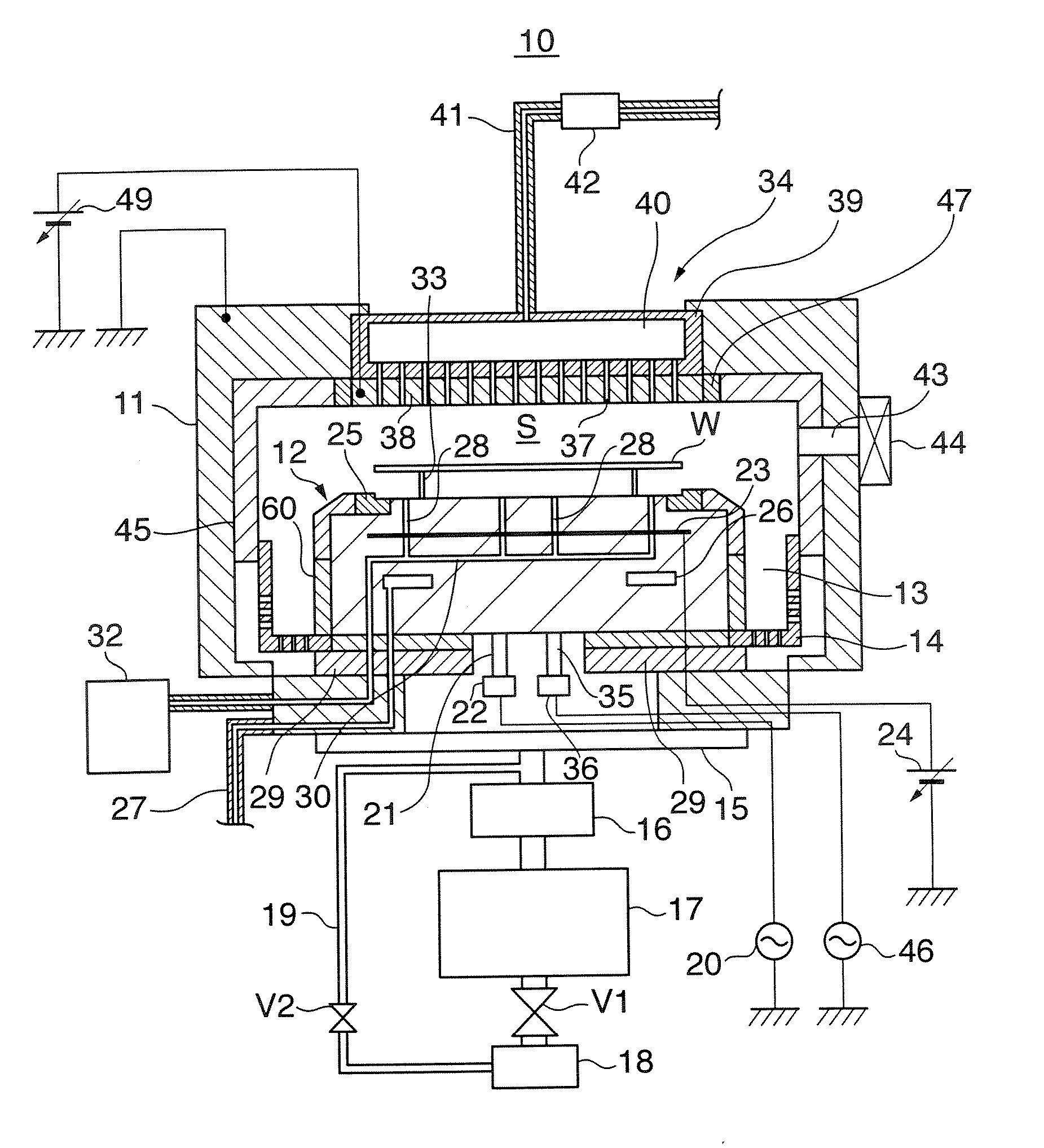
[0076] As shown in FIG. 6, first, in the plasma processing apparatus 10 in which reaction product has become attached to the surface of the upper electrode plate 38, a wafer W that has been subjected to RIE is transferred out from the substrate processing chamber 11 (step S61). Next, oxygen gas is introduced from the gas introducing shower head 34 into the processing space S (step S62), and moreover 40 MHz radio frequency electrical power is applied into the processing space S so as to produce plasma, whereby dry cleaning (attached matter removal processing) is carried out (step S63) (first plasma processing step).

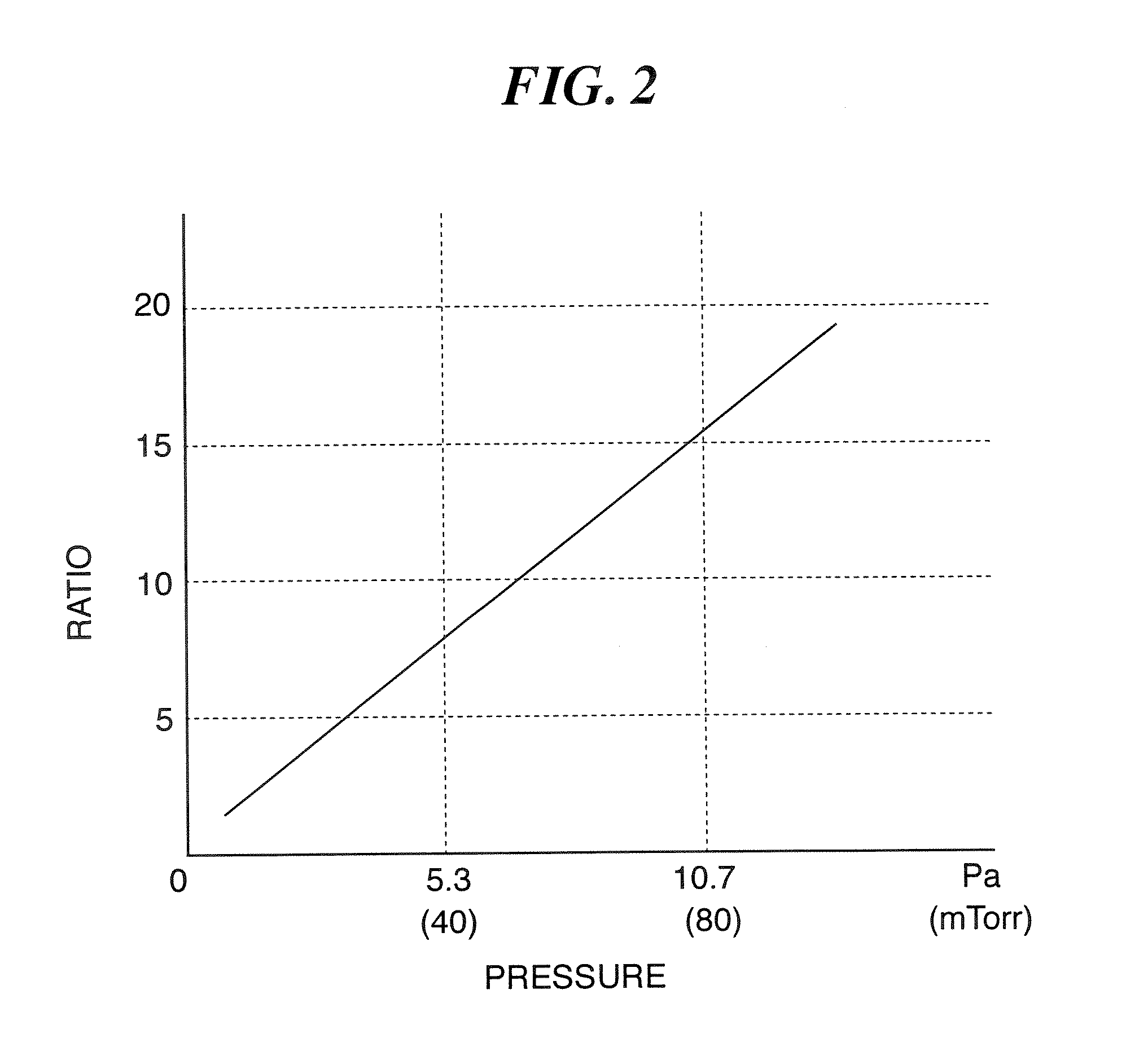
[0077] In step S63, the pressure in the processing space S is set in a range of 26.7 Pa to 80.0 Pa using the APC valve 15. The reason that the upp...

second embodiment

[0085] Next, a substrate processing chamber cleaning method according to the present invention will be described.

[0086] In the present embodiment, the construction and operation are basically the same as in the first embodiment described above, the only difference being that the pressure in the processing space S, the value of the electrode plate surface-space potential difference, and the magnitudes of the 40 MHz radio frequency electrical power and the 2 MHz radio frequency electrical power in the dry cleaning are different to in the first embodiment described above. Description of aspects of the construction that are the same as in the first embodiment will thus be omitted, only aspects of the operation that are different to in the first embodiment being described below.

[0087]FIG. 7 is a flowchart of the substrate processing chamber cleaning method according to the present embodiment.

[0088] As shown in FIG. 7, first, steps S61 and S62 are carried out as described above, and the...


PUM

PropertyMeasurementUnit
pressureaaaaaaaaaa
radio frequency electrical poweraaaaaaaaaa

Abstract

A method of cleaning a substrate processing chamber that enables formation of an oxide film on a surface of a processing chamber inside component to be prevented. A substrate processing chamber 11 has therein a processing space S into which a wafer W is transferred and carries out reactive ion etching on the wafer W in the processing space S. The substrate processing chamber 11 has an upper electrode plate 38 that comprises silicon and a lower surface of which is exposed to the processing space S. A dry cleaning is carried out on the upper electrode plate 38 using oxygen radicals produced from oxygen gas introduced into the processing space S. An oxide removal processing is carried out on the upper electrode plate 38 using fluorine ions and fluorine radicals produced from carbon tetrafluoride gas introduced into the processing space S.

Description

BACKGROUND OF THE INVENTION [0001] 1. Field of the Invention [0002] The present invention relates to a method of cleaning a substrate processing chamber, a storage medium, and a substrate processing chamber, and in particular relates to a method of cleaning a substrate processing chamber having an electrode made of silicon. [0003] 2. Description of the Related Art [0004] Plasma processing apparatuses having a substrate processing chamber having therein a processing space into which is transferred a semiconductor wafer as a substrate, and a lower electrode that is disposed in the processing space and is connected to a radio frequency power source are known. In such a plasma processing apparatus, a processing gas is introduced into the processing space, and the lower electrode applies radio frequency electrical power into the processing space. Moreover, when a semiconductor wafer has been transferred into the processing space and mounted on the lower electrode, the introduced processi...

Claims


Application Information

Patent Timeline
Patent Type & Authority Applications(United States)
IPC IPC(8): B08B6/00G06F19/00C23F1/00C23C16/00
CPCH01J37/32862B08B7/0035Y10S438/905
Inventor HONDA, MASANOBUMATSUI, YUTAKA
Owner TOKYO ELECTRON LTD
Why Eureka
Try Eureka