Modification
- Summary
- Abstract
- Description
- Claims
- Application Information
AI Technical Summary
Benefits of technology
Problems solved by technology
Method used
Image
Examples
Embodiment Construction
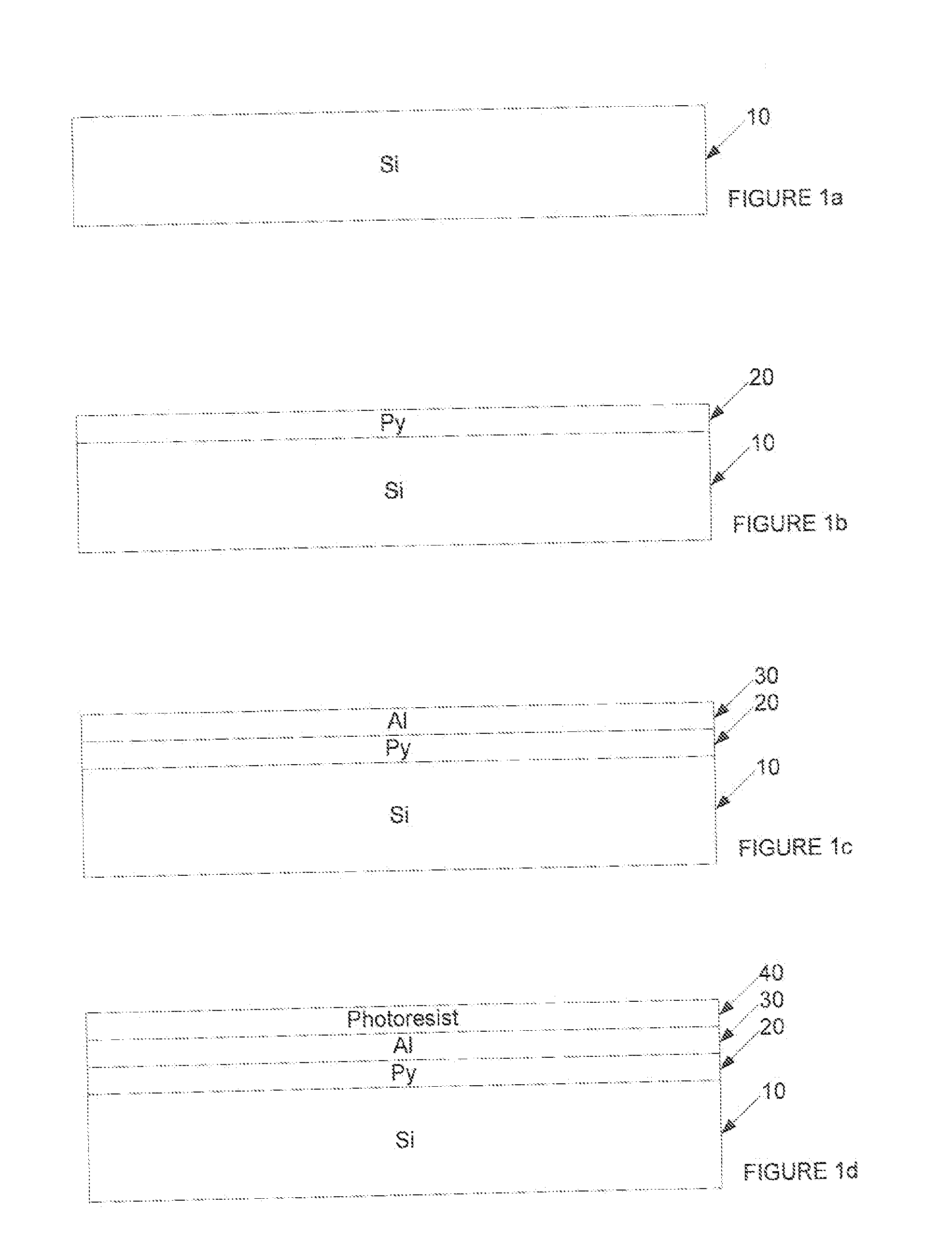
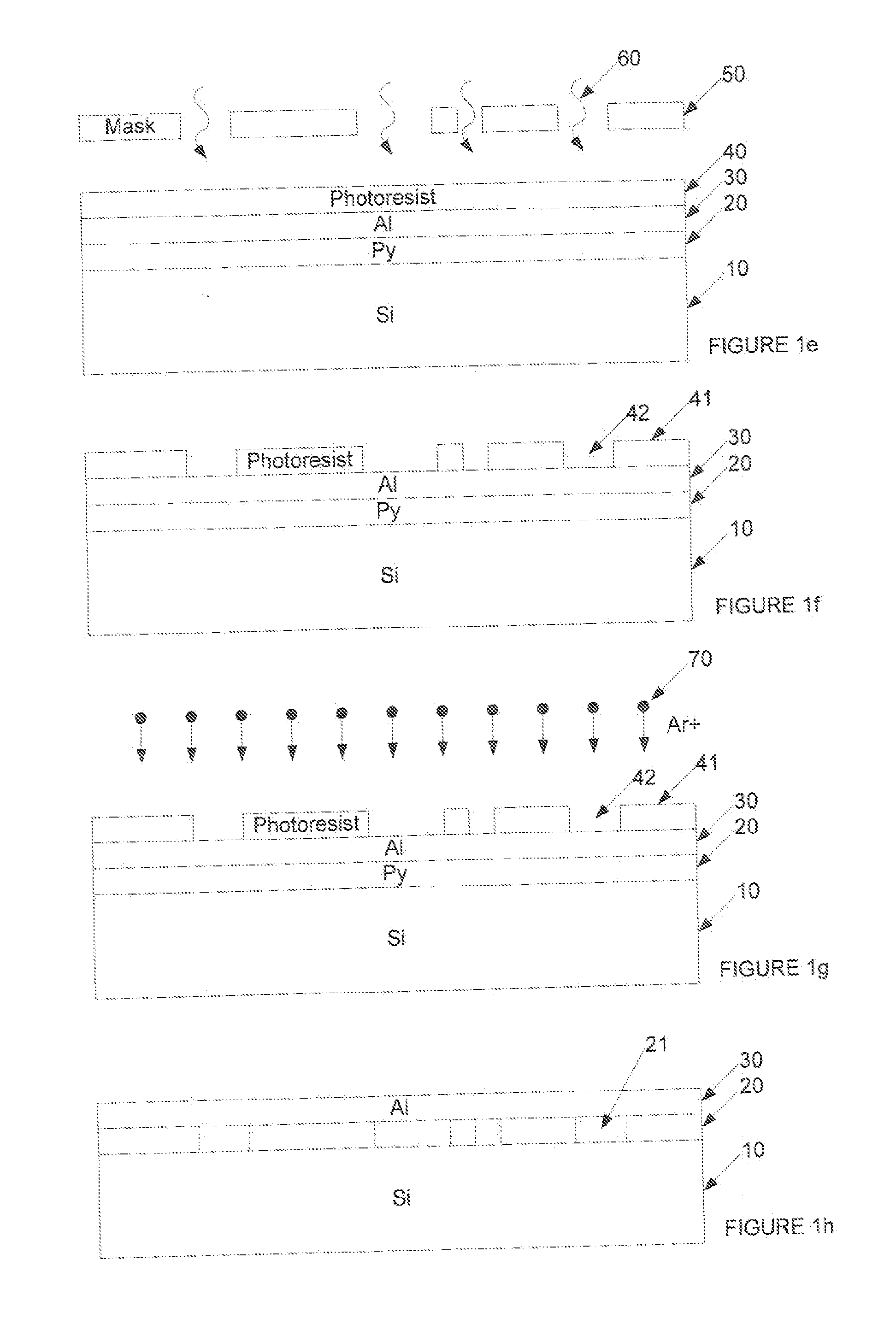
[0037] An example of a structure of patterned ferromagnetic material, and a method of manufacturing same will be described with reference to FIG. 1.
[0038] First, a substrate 10 of silicon is provided as shown in FIG. 1a. Onto this substrate 10, a thin film 20 of permalloy (Ni80Fe20) is deposited by thermal evaporation, spatter deposition or electro-deposition as shown in FIG. 1b. The thin film 20 of permalloy has, in the present example, a thickness in the range of 0.5-10 nm. A thickness in the range 2-5 nm may produce improved results.
[0039] Then, over the thin film permalloy layer 20, a surface layer 30 of Aluminium is deposited using thermal evaporation or spatter deposition as shown in FIG. 1c. This surface layer 30 has, in the present example a thickness of between one and three times the thickness of the thin film permalloy layer 20. Thus a thickness in the range 5-15 nm may produce good results.
[0040] At this stage, the permalloy layer 20 has a substantially uniform magnet...
PUM
| Property | Measurement | Unit |
|---|---|---|
| Magnetism | aaaaa | aaaaa |
| Anisotropy | aaaaa | aaaaa |
| Coercivity | aaaaa | aaaaa |
Abstract
Description
Claims
Application Information


