Semiconductor Device Having Shallow Trench Isolation and Method of Forming the Same

Inactive Publication Date: 2015-10-22
MICRON TECH INC
View PDF11 Cites 13 Cited by
  • Summary
  • Abstract
  • Description
  • Claims
  • Application Information

AI Technical Summary

Benefits of technology

The present invention relates to a method of forming dielectric films in semiconductor devices. The invention provides better protection against stress in the substrate that can lead to crystal defects. This is achieved by making the dielectric films on the bottom surfaces of trenches thicker than on the side surfaces, which results in a reduction of stress on the substrate when a second isolation film is formed.

Problems solved by technology

The progress of microfabrication in recent years has lead to an increase in the aspect ratio of trenches, which makes difficult burying a dielectric film securely in a trench.

Method used


Image

  • Semiconductor Device Having Shallow Trench Isolation and Method of Forming the Same
  • Semiconductor Device Having Shallow Trench Isolation and Method of Forming the Same
  • Semiconductor Device Having Shallow Trench Isolation and Method of Forming the Same

Examples


first embodiment

[0042]A preferred first embodiment of the present invention will hereinafter be described in detail with reference to drawings.

[0043](Semiconductor Device)

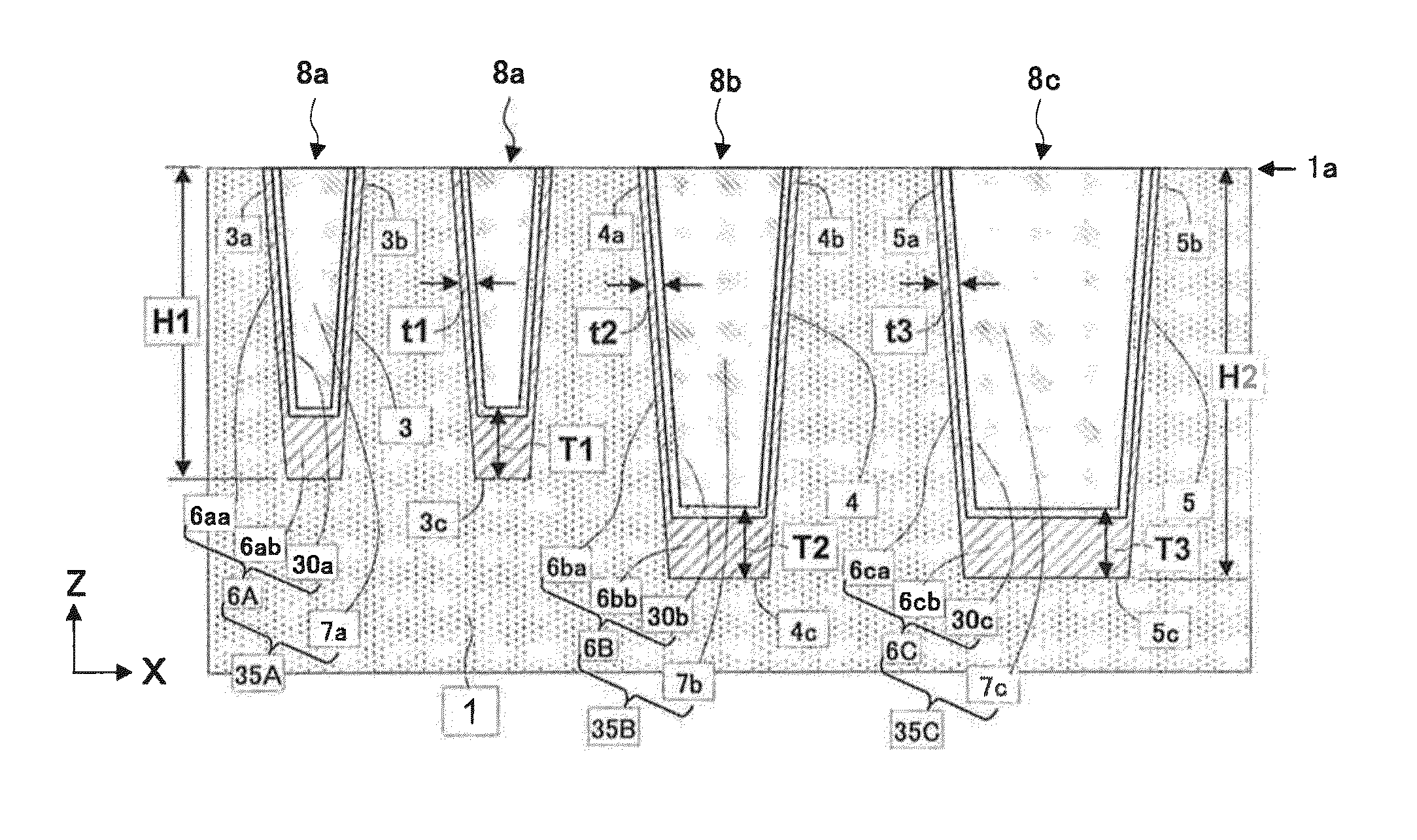
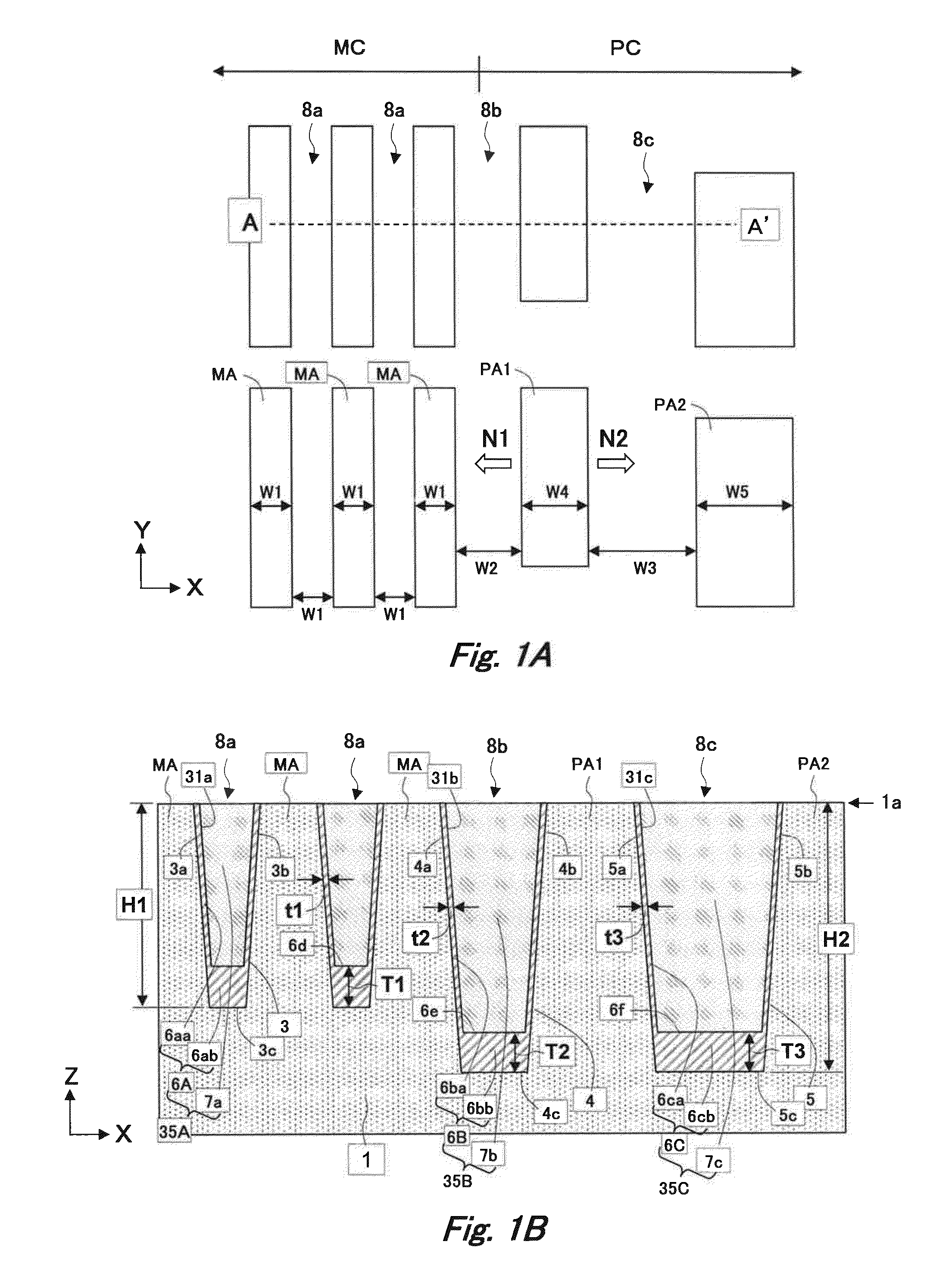
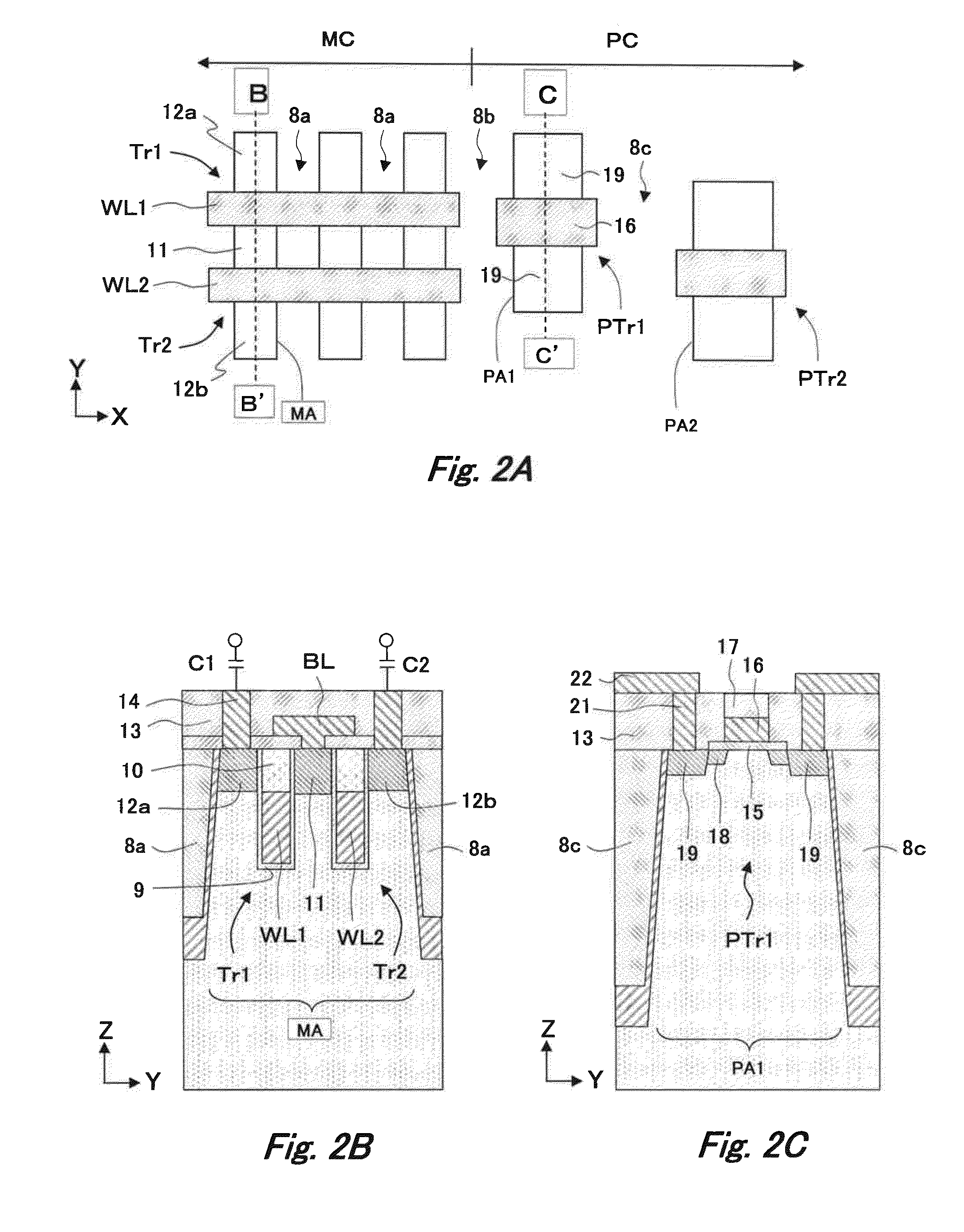
[0044]FIGS. 1A, 1B, 2A, 2B, and 2C are diagrams showing a DRAM as a semiconductor device according to preferred embodiments of the present invention. FIG. 1A is a plan view showing a layout of active areas. FIG. 1B is a sectional view along an A-A′ line of FIG. 1A. FIG. 2A is a more specific plan view of the DRAM. FIG. 2B is a sectional view along a B-B′ line of FIG. 2A. FIG. 2C is a sectional view along a C-C′ line of FIG. 2A. The semiconductor device described in the first embodiment is a semiconductor memory device, such as DRAM and NAND flash, but may be provided as other forms of devices.

[0045]The plan view of FIG. 1A will be referred to. The DRAM includes a memory cell area MC disposed on one main surface of a semiconductor substrate, and a peripheral circuit area PC for controlling and driving memory cells.

[0046]In the memo...

second embodiment

[0087]FIG. 9 is a process diagram showing a method of manufacturing the semiconductor device according to a preferred second embodiment of the present invention.

[0088]According to the first embodiment, the trenches are formed such that the depth H1 of the first trench 3 having the smallest opening width is different from the depth H2 of the second trench 4 and third trench 5 each having the opening width larger than that of the first trench 3, as shown in FIG. 1B. The method of manufacturing the semiconductor device according to the second embodiment is provided as a method by which trenches with different opening widths are so formed as to have the identical depth.

[0089]In the first embodiment, the condition for the anisotropic dry etching performed during the trench forming process specifies use of the mixed gas plasma made up of hydrogen bromide (HBO of 70 sccm, chloride (Cl2) of 70 sccm, sulfur hexafluoride (SF6) of 10 sccm, and oxygen (O2) of 20 sccm under a pressure of 20 mToo...


PUM


Abstract

A device includes a first dielectric film formed in a first trench along a first bottom surface portion and a first side surface portion with leaving a first gap in the first trench and a second dielectric film formed in a second trench along a second bottom surface portion and a second side surface portion with leaving a second gap in the second trench. The first bottom surface portion is covered approximately conformably with a first part of the first dielectric film, the first side surface portion is covered approximately conformably with a second part of the first dielectric film, and the first part is larger in thickness than the second part. The second bottom surface portion is covered approximately conformably with a third part of the second dielectric film, the second side surface portion is covered approximately conformably with a fourth part of the second dielectric film, and the third part is larger in thickness than the fourth part.

Description

BACKGROUND OF THE INVENTION[0001]1. Field of the Invention[0002]The present invention relates to a semiconductor device and a method of manufacturing the same, particularly to a semiconductor device having an STI (Shallow Trench Isolation) structure and a method of manufacturing the same.[0003]Priority is claimed on Japanese Patent Application No. 2014-084659, filed Apr. 16, 2014, the content of which is incorporated herein by reference.[0004]2. Description of the Related Art[0005]In a semiconductor device, such as DRAM (Dynamic Random Access Memory), a dielectric film is formed between elements adjacent to each other so that insulation between the elements is ensured by the dielectric film. An isolation dielectric film is formed by burying a dielectric film in a trench formed on a semiconductor substrate. The progress of microfabrication in recent years has lead to an increase in the aspect ratio of trenches, which makes difficult burying a dielectric film securely in a trench.[000...

Claims


Application Information

Patent Timeline
IPC IPC(8): H01L29/06H01L21/762
CPCH01L21/76229H01L29/0649H01L29/4236H01L29/7833H10B12/09
Inventor ISHIKAWA, SHIGEO
Owner MICRON TECH INC
Why Eureka
Try Eureka