

Electrode structure for use in electronic device and method of making same
a technology of electronic devices and electrodes, applied in the direction of sustainable manufacturing/processing, semiconductor devices, climate sustainability, etc., can solve the problems of sodium (na) dispersing into the coating in an uncontrollable and predictable manner, undesirable and/or unpredictable functionality, etc., to prevent or reduce sodium (na) migration
- Summary
- Abstract
- Description
- Claims
- Application Information
AI Technical Summary
Benefits of technology
Problems solved by technology
Method used
Image

Examples
Embodiment Construction
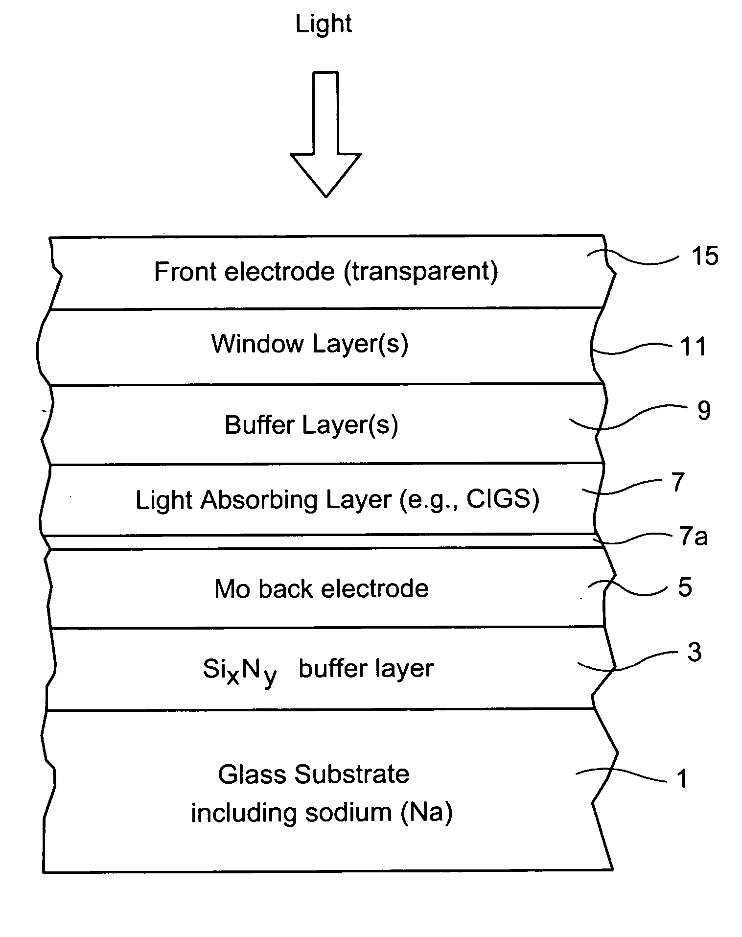
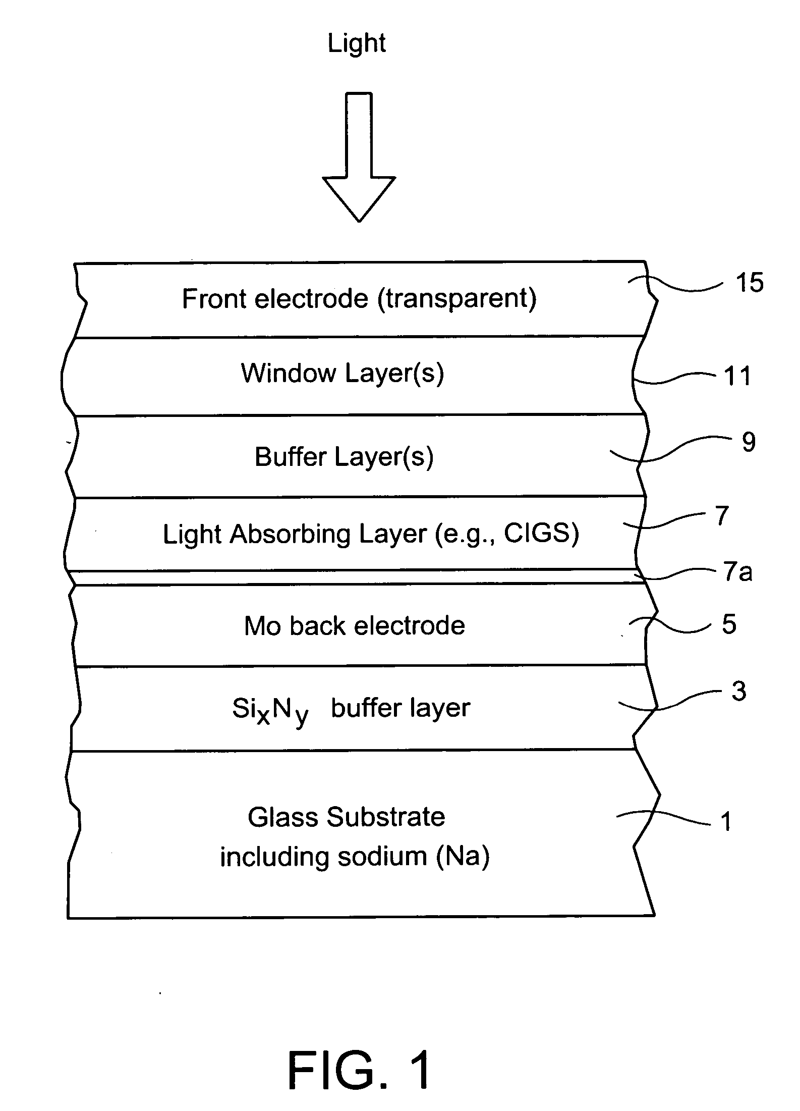
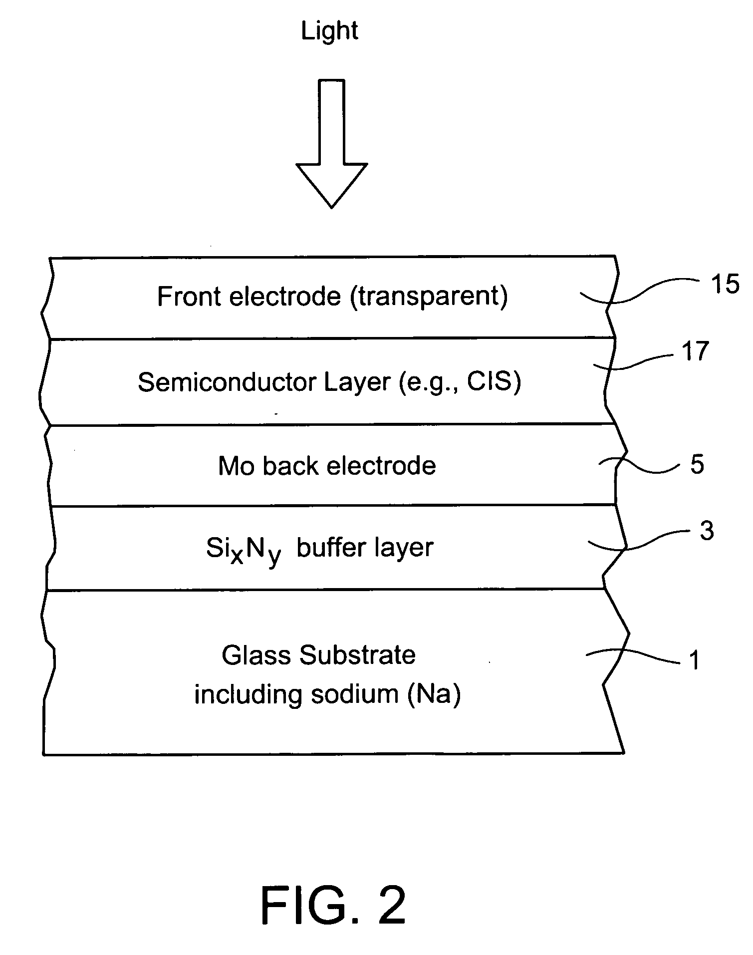
[0007] In certain example embodiments of this invention, an electrode structure is provided for use in solar cells and the like. In certain example embodiments, an electrode structure includes a supporting glass substrate (e.g., soda-lime silica based float glass), a buffer layer (e.g., SixNy), and a conductive electrode (e.g., Mo) provided in this order. The buffer layer is advantageous in that it prevents or reduces sodium (Na) migration from the glass substrate, through the Mo back electrode, and into semiconductor layer(s) of the electronic device (e.g., solar cell or other suitable electronic device). Thus, if desired, sodium may be added to the semiconductor layer from above in a post-deposition treatment (i.e., not from the glass). The buffer layer may be of silicon nitride, and may include oxygen and / or other element(s) as well in certain example embodiments of this invention. The buffer layer may be made up of a single layer or multiple layers in different example embodimen...
PUM
| Property | Measurement | Unit |
|---|---|---|
| thick | aaaaa | aaaaa |
| thick | aaaaa | aaaaa |
| thick | aaaaa | aaaaa |
Abstract
Description
Claims
Application Information