Semiconductor device

a technology of semiconductors and junctions, applied in the direction of semiconductor devices, basic electric elements, electrical equipment, etc., can solve the problems of insufficient concentration of electric fields in an end region, inability to form such a narrow-pitched super-junction structure not only in an element region, and inability to achieve high breakdown voltage in an end region

Inactive Publication Date: 2007-08-23
KK TOSHIBA
View PDF7 Cites 48 Cited by
  • Summary
  • Abstract
  • Description
  • Claims
  • Application Information

AI Technical Summary

Problems solved by technology

Thus, it is difficult to form such a narrow-pitched super-junction structure not only in an element region but also in an end region surrounding the element region.
For this reason, in a power MOS transistor with a breakdown voltage of about 30V used for an energy-saving switching element, concentration of electric field in an end region could not be eased enough.
Therefore, a breakdown voltage in an end region cannot be high enough compared to that in an element region.
This is recognized as a problem.

Method used


Image

  • Semiconductor device
  • Semiconductor device
  • Semiconductor device

Examples


first embodiment

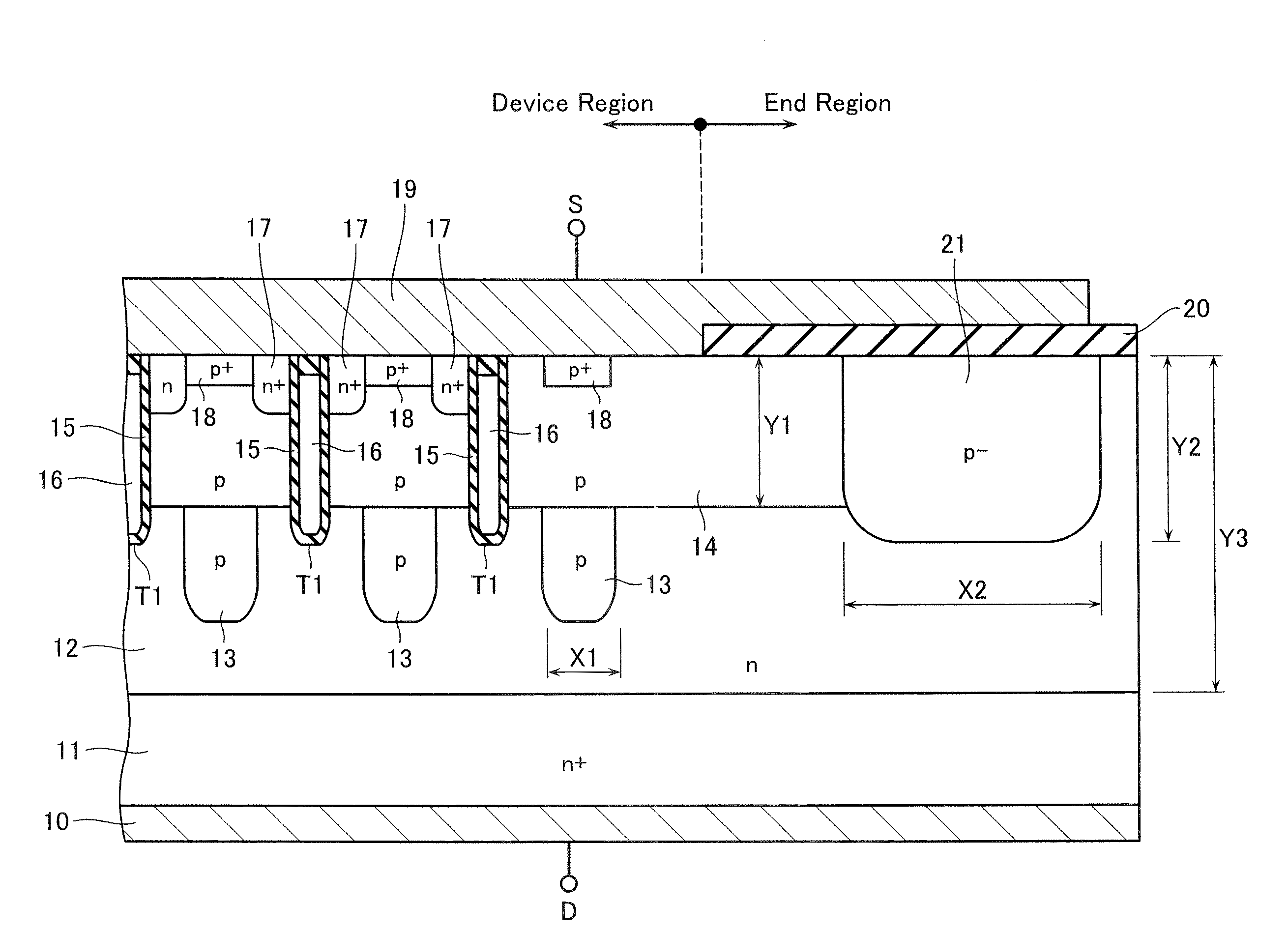
[0019]FIG. 1 illustrates a cross-sectional structure of a semiconductor device according to a first embodiment of the present invention.

[0020]This semiconductor device is composed of an element region in which a semiconductor device, for example, a so-called trench-gate type n-channel MOS transistor is formed, and an end region formed to surround this element region. AMOS transistor in this embodiment is supposed to be a MOS transistor with a breakdown voltage of about 30V for the energy-saving switching device market used on a mobile communication device. Furthermore, although a trench gate type n-channel MOS transistor is explained as an example here, the present invention may not be limited to this. It may include a p-channel MOS transistor. The present invention may be applied to an IGBT, a Schottky-barrier diode, and so forth. Moreover, the present invention is applicable also to the planer type semiconductor device instead of a trench gate type.

[0021]As shown in FIG. 1, an n-c...

second embodiment

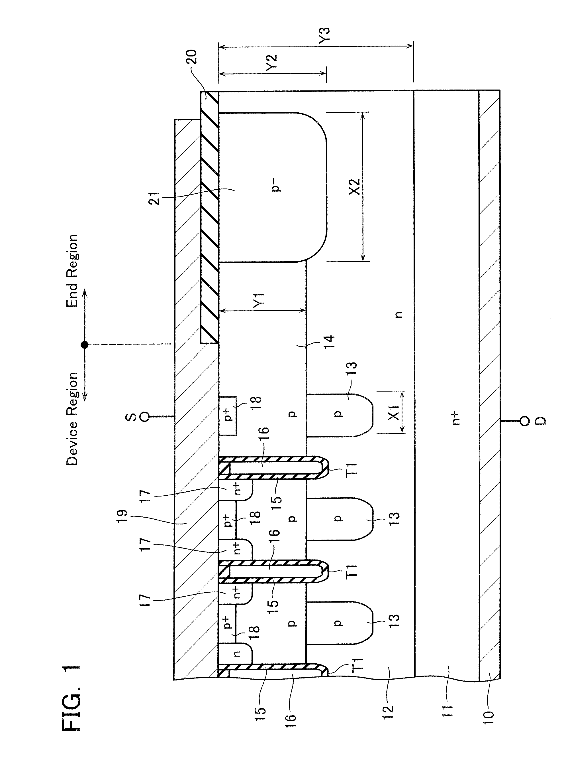
[0035]Next, the second embodiment of the present invention will be explained with reference to FIG. 3. In FIG. 3, the same numerals are given to the same components as FIG. 1, and these components have the same structures and functions. Therefore, the detailed explanation thereof is omitted hereinbelow.

[0036]This embodiment comprises an n-type embedded layer 22 under the p-type termination layer 21. This layer has an effective impurity concentration and a career concentration lower than those in the n-type epitaxial layer 12 and a high resistance. This n-type embedded layer 22 may be formed by carrying out ion implantation of boron (B) with high energy, when forming the termination layer 21. As described above, by forming the n-type embedded layer 22 with lower career concentration under the termination layer 21, a depletion layer spreads in the end region easily at the time of the non-conductive state of a MOS transistor, and it is possible to raise the breakdown voltage of the end...

third embodiment

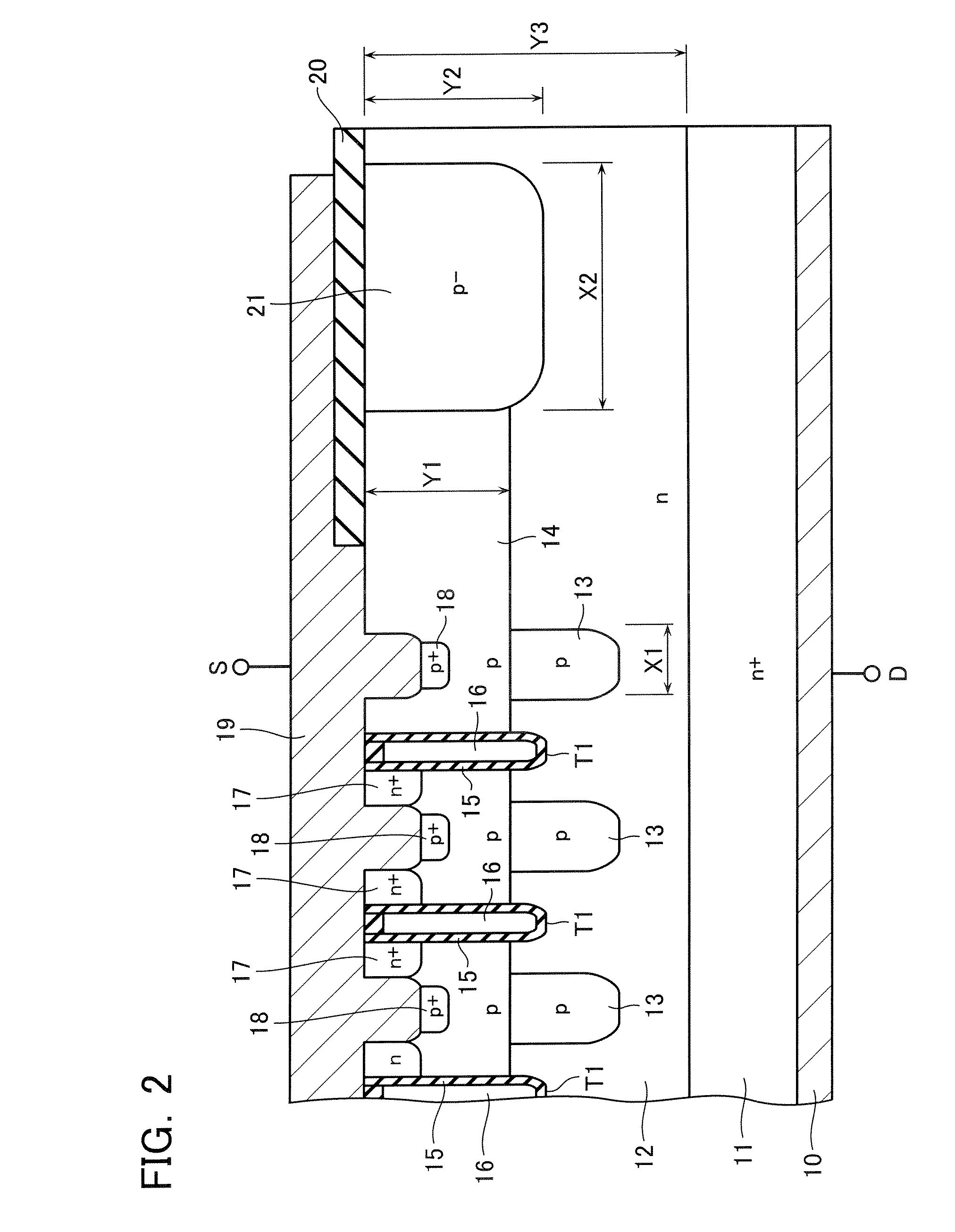
[0037]Next, the third embodiment of the present invention will be explained with reference to FIG. 4. In FIG. 4, the same numerals are given to the same components as FIG. 3, and these components have the same structures and functions. Therefore, the detailed explanation thereof is omitted hereinbelow.

[0038]This embodiment is different from the second embodiment in that the termination layer 21 is not formed in the end region, and only the n-type embedded layer 22 is formed in the bottom of the epitaxial layer 12. The p-type base layer 14 is extended to the end region. Also in this embodiment, if the career concentration of the n-type embedded layer 22 is set low, it is possible to extend a depletion layer close to the silicon substrate 11 at the time of the non-conductive state of a MOS transistor. This may maintain the breakdown voltage of the end region high enough compared to that in the element region.


PUM


Abstract

This semiconductor device comprises a first semiconductor layer of a first conductivity type, an epitaxial layer of a first conductivity type formed in the surface on the first semiconductor layer, and a base layer of a second conductivity type formed on the surface of the epitaxial layer. Column layers of a second conductivity type are repeatedly formed in the epitaxial layer under the base layer at a certain interval. Trenches are formed so as to penetrate the base layer to reach the epitaxial layer; and gate electrodes are formed in the trenches via a gate insulation film. A termination layer of a second conductivity type is formed on the epitaxial layer at an end region at the perimeter of the base layer. The termination layer is formed to have a junction depth larger than that of the base layer.

Description

CROSS REFERENCE TO RELATED APPLICATIONS[0001]This application is based on and claims the benefit of priority from prior Japanese Patent Application No. 2006-41954, filed on Feb. 20, 2006, the entire contents of which are incorporated herein by reference.BACKGROUND OF THE INVENTION[0002]1. Field of the Invention[0003]The present invention relates to a semiconductor device, more particularly to a semiconductor device including a so-called trench gate type MOS transistor.[0004]2. Description of the Related Art[0005]In recent years, demands of power MOS transistors are increasing rapidly, not only in a market of switching power supplies with large current and high breakdown voltage (for example, a breakdown voltage of 600V), but also in a market of energy-saving switching devices used in a mobile communication device including a notebook PC (for example, a breakdown voltage of 30V).[0006]A power MOS transistor used in such an energy-saving switching device market is required to reduce i...

Claims


Application Information

Patent Timeline
Patent Type & Authority Applications(United States)
IPC IPC(8): H01L29/94
CPCH01L29/0615H01L29/0634H01L29/1095H01L29/7813H01L29/41741H01L29/41766H01L29/7811H01L29/402
Inventor KAWAGUCHI, YUSUKEYAMAGUCHI, YOSHIHIROONO, SYOTAROAKIYAMA, MIWAKO
Owner KK TOSHIBA
Why Eureka
Try Eureka